Overall Design Scheme for ZYNQ MPSoC-Based Image Acquisition and Compression System
2.1 Introduction
In flight missions, high-definition video data has become a critical basis for analyzing flight status and evaluating system performance. However, the massive data volume generated by 4K ultra-high-definition video poses significant challenges to acquisition, processing, and storage systems. An uncompressed 4K@60Hz video stream produces approximately 12 Gbit of data per second. Without effective compression, such data becomes difficult to transmit in real time or store long-term.
Therefore, based on mission requirements, this paper presents the design of an image processing system capable of acquiring and compressing multiple high-definition video streams. The system must support real-time acquisition, processing, H.265 compression, and multi-path output of 4K@60Hz video, along with precise timestamp watermarking functionality.
2.2 Requirement Analysis and Technical Specifications
According to the mission specifications, the image acquisition and compression system must acquire, store, and compress multiple 4K@60Hz video data streams while supporting various interface outputs. The main technical requirements are as follows:
- Video Input: Support four video input channels with a multiplexer configuration (select one from multiple inputs).
- Video Parameters: Support video compression up to 4K@60Hz, with configurable resolution and frame rate.
- Timing Accuracy: Implement hardware timestamping at the front end of the acquisition chain for stored image data.
- Video Output:
- Support local storage with playback capability.
- Provide LVDS interface output to external storage modules for backup and redundancy management.
- Enable real-time PCM output.
- Support RTP-based network transmission for synchronized real-time playback.
- Allow command-controlled video compression parameters such as resolution and frame rate.
2.3 Video Processing Architecture Selection
Based on the requirements and technical specifications outlined in Section 2.2, the goal of the video processing system is to fully realize the functionality of receiving multiple video streams, encoding and compressing them, and then saving and outputting the data. Grounded in three core design principles—multi-channel input, minimal latency, and intelligent processing—the architecture must carefully consider the following key aspects:
(1) Sufficient user I/O (input/output) interface availability;
(2) Diverse peripheral interface resource allocation;
(3) Complete processing system architecture supporting upper-layer application development;
(4) High-performance video codec modules for data stream compression;
(5) Dedicated image processing units supporting execution of image analysis algorithms.
Considering these five factors along with current market application trends, two video processing solutions can be considered:
(1) Discrete Architecture
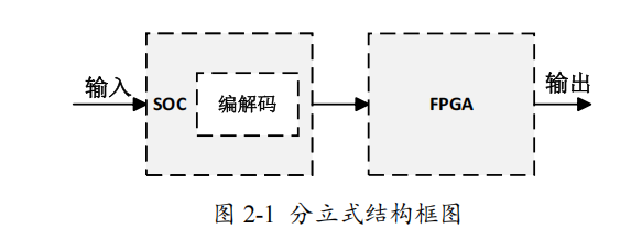
This approach uses a collaborative mechanism between an FPGA (Field-Programmable Gate Array) and a SoC (System-on-Chip) codec chip. In this architecture, the FPGA primarily handles output of multi-format interface image data and parallel processing of interface command information, while the SoC manages embedded system development, establishing communication channels between the underlying hardware and upper-layer software to complete video acquisition, compression, and decompression. The discrete architecture is illustrated in Figure 2-1.
(2) Integrated MPSoC Architecture
This solution leverages the integrated programmable logic (PL) and processing system (PS) of Xilinx ZYNQ UltraScale+ MPSoC devices. The PL handles high-speed interface processing and real-time image operations, while the PS runs embedded Linux to manage system control, configuration, and application logic. The built-in Video Codec Unit (VCU) supports hardware-accelerated H.265/HEVC encoding and decoding, enabling efficient compression of 4K@60Hz video. This architecture offers superior integration, lower latency, and higher processing efficiency, making it ideal for high-performance video applications.
Given the need for high integration, low latency, and real-time processing capability, the integrated MPSoC architecture is selected as the foundation of this design.
2.4 HDMI Input Architecture Selection
Based on the requirements in Section 2.2, the goal of the video acquisition system is to effectively process received HDMI 4K@60Hz video data and transmit it to the backend system. Guided by three core design principles—high resolution, minimal latency, and efficient resource utilization—the HDMI acquisition solution must address the following considerations:
(1) Support acquisition of 4K@60Hz high-resolution HDMI signals;
(2) Provide sufficient bandwidth to meet high-speed data transmission requirements;
(3) Use system I/O resources efficiently;
(4) Achieve high integration to reduce hardware complexity;
(5) Offer strong data processing flexibility for future expansion.
Considering these factors and current technological capabilities, two HDMI acquisition approaches are evaluated:
(1) External HDMI Decoder Chip
This approach uses a dedicated HDMI decoder chip connected to the PL portion of the MPSoC, as shown in Figure 2-3. The HDMI decoder chip receives differential HDMI signals, decodes them into parallel RGB data format, and transfers the data via a parallel bus to the MPSoC’s PL for further processing.
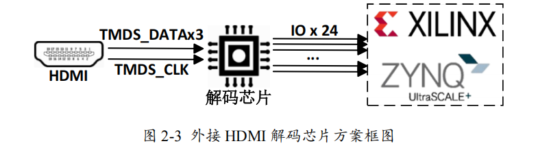
This solution offers a mature design with well-defined interfaces and moderate development difficulty. However, it has notable limitations for 4K@60Hz signals:
- Commonly available HDMI decoder chips (e.g., MS7200) often fail to fully support the high bandwidth required by 4K@60Hz, typically supporting only up to 4K@30Hz or lower;
- Parallel RGB output consumes significant FPGA I/O resources—approximately 12 Gbps for 24-bit color depth at 4K@60Hz, leading to substantial pin usage;
- Additional HDMI decoder chips increase system power consumption, PCB area, and complexity;
- Signal integrity becomes more challenging, requiring careful timing and impedance matching for high-speed parallel buses.
(2) Direct HDMI Differential Signal Connection to GTH Interface
This solution directly connects the HDMI differential signals to the GTH high-speed transceivers of the MPSoC, as illustrated in Figure 2-4. The GTH transceivers receive the high-speed serial HDMI signal, and HDMI protocol parsing and image processing are implemented within the PL fabric.
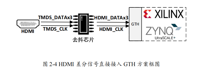
This approach offers significant advantages:
- The GTH transceivers support data rates up to 33 Gbps, fully meeting the 18 Gbps bandwidth required by HDMI 2.0 for 4K@60Hz video;
- Direct use of GTH interfaces reduces I/O resource usage by approximately 80% compared to parallel RGB transmission;
- Higher integration reduces the number of external components and PCB routing complexity;
- Built-in equalizers and clock recovery circuits in GTH transceivers improve signal integrity in high-speed transmission;
- Custom HDMI protocol parsing and image processing algorithms can be flexibly implemented in the PL, enhancing system flexibility.
From a performance perspective, Solution (2) is better suited for 4K@60Hz video acquisition. The external decoder chip approach faces clear bandwidth bottlenecks and struggles to meet the strict demands of high-resolution, high-refresh-rate video, whereas the GTH direct acquisition method easily handles the full data throughput of HDMI 1.4/2.0 standards with its 33 Gbps capability.
From a resource utilization standpoint, the GTH-based solution significantly reduces I/O footprint. Parallel RGB transmission would require numerous FPGA pins for 4K@60Hz video, while the GTH solution achieves the same function with only a few high-speed differential pairs, freeing I/O resources for other system functions.
Regarding signal integrity, high-speed differential signaling offers superior noise immunity and reliability compared to wide parallel buses. The built-in signal conditioning and recovery features of GTH transceivers further enhance transmission stability, ensuring reliable 4K video capture.
In terms of system flexibility, Solution (2) enables direct HDMI protocol processing in the PL, allowing customization and optimization based on application needs—including protocol parsing, image preprocessing, and feature extraction—laying the foundation for future functional expansion.
In summary, the direct HDMI differential signal connection to GTH interfaces demonstrates clear advantages in performance, resource utilization, integration, signal integrity, and flexibility. Therefore, this design selects Solution (2) as the final implementation for 4K@60Hz HDMI video acquisition.
2.5 Overall System Architecture
Based on the system requirements and technical specifications in Section 2.2 and the video processing architecture selection in Section 2.3, the overall hardware architecture of the system is shown in Figure 2-5. It consists of three main components: video acquisition, video processing, and video output. The video acquisition section includes four HDMI interfaces. The acquired ultra-high-definition video is processed in real time, including HDMI decoding, image scaling and frame rate conversion, H.265 compression, and timestamp watermarking. After processing, the video can be output via multiple interfaces including Ethernet, LVDS, RS422, and SD card, depending on application needs.
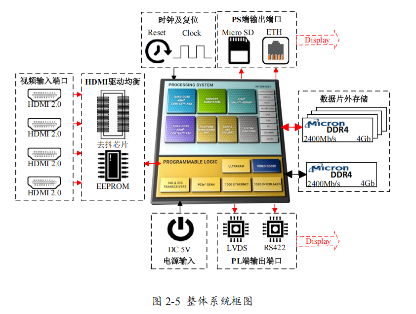
The video acquisition module provides four HDMI 2.0 interfaces, supporting simultaneous input of multiple 4K@60Hz video signals. A programmable multiplexer enables selection from multiple inputs. Each HDMI interface supports up to 18 Gbps bandwidth, fully meeting the transmission requirements of 4K@60Hz video with 24-bit color depth. The module incorporates dedicated video signal driving and equalization circuits to ensure stable acquisition of high-quality video even in complex environments.
The HDMI signals enter the FPGA through GTH high-speed differential interfaces and are processed by the Video PHY Controller at the physical layer. The HDMI Receiver Subsystem then parses the HDMI protocol to extract video and control data. After pixel clock domain conversion, the video data is formatted as AXI4-Stream for internal system transmission.
The video processing module serves as the core processing unit, responsible for a series of operations including preprocessing and compression of the raw video data. The module first uses the VPSS (Video Processing Subsystem) for video preprocessing functions such as color space conversion (e.g., RGB to YUV), resolution scaling, deinterlacing, and frame rate conversion. The VPSS employs a pipelined architecture and supports real-time processing up to 8K resolution, providing high-quality video input for subsequent encoding.
A high-precision timestamp watermarking function is implemented using AXI-BRAM. The system sends time request commands to the PL via the AXI-BRAM interface. The PL-side timing module generates precise time information and returns it to the PS via interrupt mechanism. The processed timestamp is overlaid onto video frames as text watermark using GStreamer’s textoverlay element, ensuring every frame carries accurate time marking—critical for post-mission data analysis.
Video encoding uses the H.265/HEVC standard, executed by the VCU (Video Codec Unit) hardware block embedded in the MPSoC. The VCU supports real-time encoding up to 4K@60fps, offering approximately 50% higher compression efficiency than H.264. Encoding parameters such as bitrate control mode, quantization parameters, GOP structure, and reference frame settings can be dynamically adjusted to balance compression ratio and image quality. Zero-copy techniques are employed during encoding to avoid performance degradation from excessive data movement, thereby improving encoding efficiency.
An efficient memory management strategy is implemented using buffering and DMA transfers to ensure continuous video processing. A custom DMA controller implemented in FPGA enables data transfer at speeds approaching the memory bandwidth limit, satisfying the high-bandwidth demands of real-time 4K video processing.
The video output module supports multiple data output methods, ensuring system versatility and high reliability. Four primary output paths are designed to meet diverse application scenarios:
- Local Storage: Compressed H.265 video is saved via SD card interface.
- LVDS Output: A dedicated LVDS driver chip transmits the compressed H.265 bitstream to an external storage module for data backup and redundant storage.
- RS422 Output: Converts video data into PCM-encoded data streams compliant with the IRIG 106 standard.
- Network Streaming: Implemented via Gigabit Ethernet interface, supporting multiple streaming protocols including RTP, RTSP, and HLS for direct network distribution of compressed video.
The network transmission module includes QoS (Quality of Service) mechanisms to prioritize video data transmission under limited bandwidth conditions. The system also supports both multicast and unicast transmission modes to accommodate different network environments.