Design of an Ultra-HD Real-Time Image Acquisition and Compression System Based on ZYNQ MPSoC ARM+FPGA
3.1 Overview of Overall Hardware Solution
Based on the analysis of system architecture and方案 in Sections 2.1 and 2.2, this chapter provides a detailed introduction to the system's hardware design. The hardware block diagram of the high-performance real-time video acquisition and compression platform described in this paper is shown in Figure 3-1. The system consists of a core processing module, a video capture module, an off-chip data storage module, a video compression data output module, a power module, a clock and reset module, and other MPSoC peripheral interfaces.
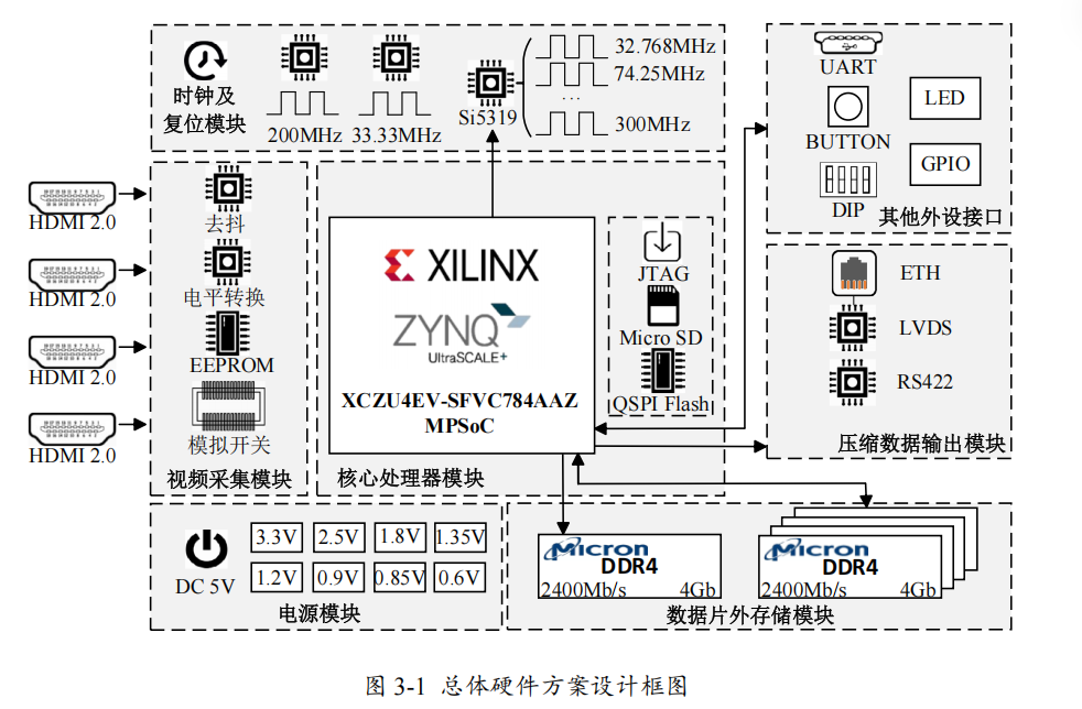
The board's video capture module features four HDMI 2.0 receiver ports capable of supporting 4K (3840×2160) resolution video input at a 60Hz refresh rate. High-speed differential video signals are passed through de-jittering and level-shifting chips before being transmitted to the system's core—the ZYNQ MPSoC processing chip. The hardware platform uses Xilinx's XCZU4EV-2SFVC784 model from the ZYNQ Ultrascale+ MPSoC EV series as the central processing unit. In addition, the processor section integrates a JTAG debugging interface, two 8-bit-wide 128 Mbit NOR Flash memory units, and a Micro SD card slot with associated circuitry, forming three boot modes for the system: the JTAG interface is primarily used for Vivado ILA testing, the Flash is responsible for storing the firmware, and the SD card in the video capture and compression system is mainly used to store BOOT.BIN and the file system. The core processing module connects to the off-chip data storage module, where the PL logic side is equipped with a 2400 MHz DDR4 memory chip with a total capacity of 4 Gb, used to buffer video data during the image pre-processing stage. On the PS processor side, four DDR4 memory chips, each operating at 2400 MHz and totaling 4 Gb in capacity, support the operation of the Petalinux operating system and provide buffer space for compressed video data. Connected to the video data output module, the system uses RS422 chips, LVDS drivers, and a Gigabit Ethernet interface to enable data exchange with external devices. Additionally, peripheral interfaces provide UART, buttons, switches, LEDs, and GPIO for system debugging assistance.
The power, clock, and reset modules ensure the normal operation of the entire system. The power supply adopts a distributed architecture, using a single 5V input and generating nine different voltage levels across 23 independent power channels via multiple DC-DC converter chips to meet the power requirements of various functional modules. The timing and reset module integrates quartz crystal oscillators of required frequencies and supports manual reset via external buttons, facilitating operational control during system debugging.
3.2 MPSoC Minimal System Principle Design
3.2.1 Core Processor Module Design
According to the system方案, the main control chip selected is the Zynq UltraScale+ MPSoC EV series from Xilinx. Among the three different variants in the EV series, the PS-side interfaces and VCU capacity are identical, while the PL-side programmable logic, memory, and integrated IP (Intellectual Property Core) resources differ. To avoid unnecessary resource waste and increased cost, a base-level chip is sufficient. The specific model used is XAZU4EV-2SFVC784, which has 784 pins. Different types of I/Os are divided into several Banks with independent power supplies to facilitate peripheral connection allocation. The pin distribution is shown in Figure 3-2.
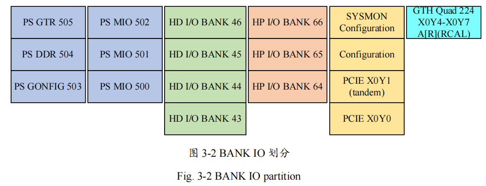
As shown in Figure 3-2 above, the ZYNQ UltraScale+ MPSoC EV processor series divides its input/output interface units (I/O Banks) into 10 different categories:
(1) HP Bank: High-performance Bank, designed specifically to meet interface performance requirements between high-speed memories and other integrated circuits. This interface supports a maximum operating voltage of 1.8V, with LVDS signal transmission rates up to 1.6 Gbps [45];
(2) HD Bank: High-density Bank, supporting high-density IO standards. Used in low-speed I/O scenarios, it supports a maximum voltage of 3.3V and data rates below 250 Mb/s, and also supports LVDS signaling standards [46];
(3) PS CONFIG 503: Processing System Configuration Bank. Used to boot the PS side and configure the PL side, supporting both secure and non-secure boot modes;
(4) PS DDR 504: Processing System DDR Memory Interface. Provides 32-bit or 64-bit interfaces for connecting DDR4, DDR3, DDR3L, or LPDDR3 memory, and a 32-bit interface for LPDDR4 memory;
(5) PS GTR 505: Processing System Multi-Gigabit Transceiver Interface. Integrates four dedicated PS-GTR transceivers supporting data rates up to 6.0 Gb/s, compatible with SGMII tri-speed Ethernet, PCI Express® Gen2, Serial ATA (SATA), USB 3.0, and DisplayPort;
(6) PS MIO: Processing System Multiplexed I/O. Can be flexibly configured into various communication standards, including SPI and Quad-SPI flash controllers, NAND memory interfaces, USB data transfer, Ethernet communication, SDIO card control, UART serial communication, standard SPI, and general-purpose GPIO. This interface group supports a maximum operating voltage of 3.3V.
(7) GT Bank: Gigabit Transceiver, representing high-speed transceivers. Implemented as power-optimized GTH transceivers in the UltraScale architecture. These interfaces support data rates from 500 Mb/s to 16.375 Gb/s, primarily used in high-bandwidth data exchange designs such as PCIe bus connections, SFF small form-factor optical interfaces, SFP+ enhanced optical modules, XAUI extended interfaces, and SATA storage interfaces.
(8) SYSMON Configuration: Responsible for system monitoring. Used to monitor FPGA internal temperature and supply voltage, and can also interface with analog signals to function as an ADC.
(9) Configuration: Responsible for PL-side configuration functions, such as loading the PL configuration bitstream, initialization, configuration interfaces, and certain PL-side IO attributes.
(10) PCIE4 Block: PL-side PCIe integrated block. Used to enumerate PCIe devices and assign corresponding addresses.
Based on the performance parameters of the above Bank types, system functionality is partitioned accordingly. During actual pin planning and circuit construction, multiple factors must be comprehensively considered, including available pin count, signal voltage specifications, data transfer rates, and layout convenience. The pin assignment for the core processor in this system is shown in Figure 3-3.
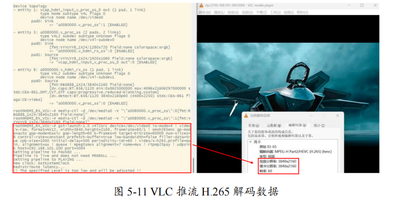
After completing the system design, performance validation is required to ensure that the design meets the specified performance requirements. Therefore, this chapter focuses on software debugging and hardware verification of each system function, including video capture testing, H.265 compression and local storage testing, real-time compressed stream playback testing, timestamp processing, and PL-side post-processing of compressed data output testing. A test and debugging system for the image acquisition and processing system was set up, consisting of a dedicated computer, hardware board, test cables, and network cables. Test method: Use dedicated host software to send control commands and receive image data; use Vivado's embedded logic analyzer (ILA) to capture, analyze, and debug powered-up devices; and directly use the host software to play back real-time video streams.
5.1 System Environment Setup
The video capture and compression system's hardware is built around the Zynq UltraScale+ MPSoC to form a complete test system. The system includes:
(1) A PC with Windows 10 and a virtual machine: used to build Vivado and Petalinux projects, compile and run environments, and deploy host software for communication with the board;
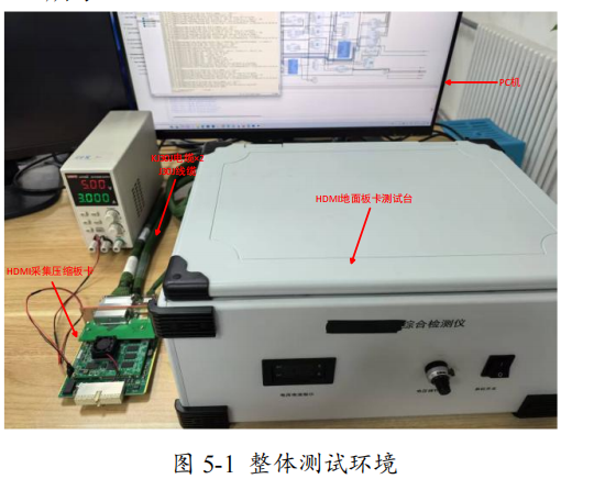
(2) Hardware board and cables: the board is fabricated according to the hardware design in Chapter 3, providing the hardware platform for experiments; KJ30J cables (for receiving 4K@60Hz HD video), CPCI connectors (for transmitting LVDS data), and J30J cables (for transmitting PCM data);
(3) Boot conditions: 5V power input and an SD card (for Petalinux system storage). The overall test environment setup is shown in Figure 5-1.
5.3.3 PS-PL Interaction Testing
(1) AXI-BRAM Interaction Test
In practical applications, AXI-BRAM is primarily used to transfer small amounts of data, such as timestamp requests and transmissions, and control command reception and acknowledgments. Therefore, this section focuses on testing timestamp and command interactions. When the image compression pipeline detects a frame, it sends a fixed request command PS2PL_DATA to the PL side via the AXI-BRAM interface and generates a request pulse PS2PL_DATA_VALID, indicating that the current timestamp request is valid. Upon receiving this, the external timing module returns the current synchronized time data PL2PS_DATA and generates an interrupt signal to notify the PS side to read the valid data from AXI-BRAM. The PL side uses ILA to capture the AXI-BRAM timestamp data interaction as shown in Figure 5-12.
The AXI-BRAM timestamp data interaction sequence on the PS side is: send timestamp request, wait for PL-side interrupt to trigger the receive process, PS-side interrupt receives and parses the timestamp data. As shown in Figure 5-13, the system log details the PS-side initialization and data interaction process. The PS side first initializes various memory mappings, successfully mapping the PL-to-PS BRAM (address 0xffff92f3c000), PS-to-PL BRAM (address 0xffff92f3a000), and PL BRAM control registers (address 0xffff92f39000). Then, the BRAM monitoring thread is started to monitor control commands in the BRAM. Once the image compression pipeline is established, the system immediately sends a timestamp request command to the PL side via BRAM.