Domestic Virtual Instruments: Zynq-based Radar 10Gbps High-Speed PCIe Data Acquisition Card Solution (Part 2) Hardware Design
This article details the hardware design of a Zynq-based 10 Gbps PCIe radar data acquisition card, covering chip selection, power architecture, clock distribution, high-speed interfaces, DDR3 memory, and the design of both the ADC daughter card and fiber-optic daughter card. Engineers working on FPGA-based data acquisition systems will find a practical reference for how to partition carrier-board and daughter-card responsibilities, select appropriate power management ICs, and configure the Xilinx Zynq-7100 SoC for high-throughput signal capture.
3.1 Introduction
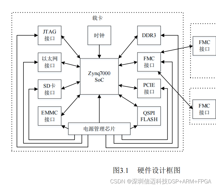
The hardware design of the acquisition card is the foundation for realizing its capture functions. A well-conceived hardware design makes the acquisition feature easier to implement and streamlines subsequent software development. This chapter builds on the hardware architecture described in Chapter 2 and provides a detailed walkthrough of chip selection, configuration, and specific circuit design for both the carrier board and the daughter cards. The overall block diagram for the carrier board and daughter cards is shown in Figure 3.1.
3.2 Carrier Board Hardware Design
3.2.1 Main Control Chip Selection and Configuration Circuit
(1) Chip Selection and Analysis
Based on the hardware design analysis from Chapter 2, the main control chip must satisfy the following requirements:
- At least 12 pairs of high-speed GTX transceivers — 4 pairs for fiber optic links and 8 pairs for PCIe.
- Sufficient on-chip BRAM resources to implement FIFO buffering at the data interfaces.
- Native support for the Aurora serial protocol and PCIe 2.0.
- General-purpose peripheral interfaces (Ethernet, SPI, UART, CAN) for ease of debugging and porting.
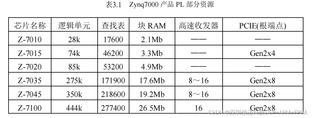
Considering all of these constraints, the design selects a chip from the Xilinx Zynq-7000 SoC family. The Zynq-7000 series integrates a dual-core ARM Cortex-A9 processing system (PS) with a Xilinx Kintex-7 FPGA programmable logic (PL) fabric on the same die, giving both hard-processor control and high-speed programmable I/O in one package. After comparing the resource tables for the product family (Table 3.1), any device at the Zynq-7135 or below can meet the design's requirements. The final selection is XC7Z100FFG900-2 from the Zynq-7100 sub-family.
The XC7Z100FFG900-2 IOBANK layout (Figure 3.2) is organized as follows:
- Bank 9–13, 33–35 — PL-side general I/O pins.
- Bank 109–112 — PL-side high-speed GTX transceivers; each bank provides four pairs of high-speed differential transceivers.
- Bank 500–502 — PS-side pins, providing standard interfaces such as Gigabit Ethernet, SPI, CAN, and UART.
White squares in the diagram represent power, ground, or configuration pins.
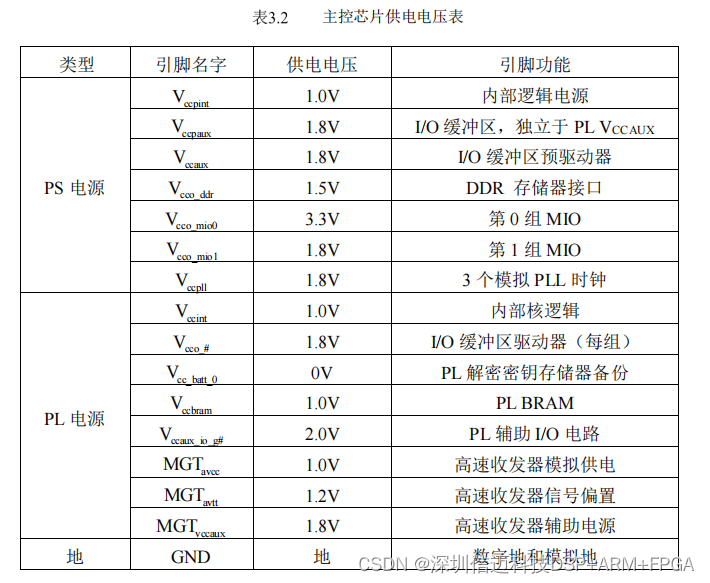
(2) Power Supply Configuration Circuit
The Zynq-7100FFG900 PL and PS sections each require different I/O supply voltages depending on bank type and performance class. PL banks are divided into HR (High Range) and HP (High Performance) categories:
- HR banks (9–13): support I/O voltages from 1.2 V to 3.3 V.
- HP banks (33–35): support I/O voltages from 1.2 V to 1.8 V only.
Beyond I/O voltages, the PL fabric also needs a core supply, an auxiliary supply, a GTX transceiver core supply, and a GTX termination supply. The PS side requires its own internal voltage, auxiliary voltage, and MIO voltage rails. The full supply voltage breakdown is summarized in Table 3.2.
(3) Clock Configuration Circuit
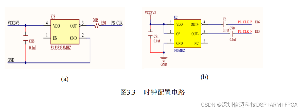
The clock distribution circuit is another critical configuration element in the Zynq-7000 design. All timing and control signals are derived from external clock references; excessive clock jitter or drift degrades overall system performance and can cause the system to stop functioning entirely. Active crystal oscillators are used as clock sources throughout.
The Zynq-7000 family has three distinct clock domains:
- PS clock: provided by a 33.333333 MHz active oscillator with a single-ended output.
- PL clock: provided by a 100 MHz active oscillator with a differential output.
- High-speed GTX clock: frequency is protocol- and data-rate-dependent and is generated by a programmable clock chip.
The PS and PL clock circuits are shown in Figure 3.3(a) and 3.3(b) respectively.
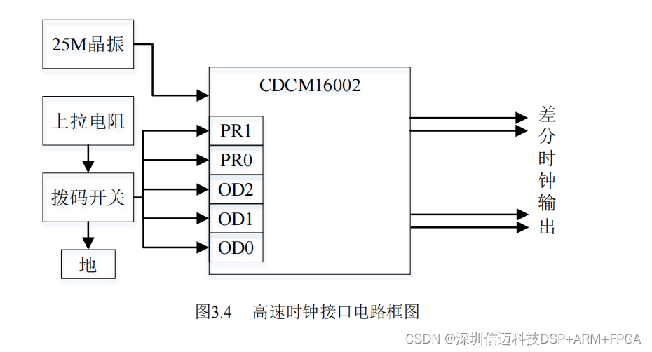
Because high-speed protocols operate at a variety of line rates, the GTX reference clock frequency must be configurable. This design uses the TI CDCM61002 programmable clock IC, which accepts a single-ended input in the range of 21.875–28.57 MHz, locks an internal high-performance VCO running at 1.75–2.05 GHz, and outputs the VCO divided by 1, 2, 3, 4, 6, or 8. It provides two pairs of differential output clocks and supports both LVCMOS and LVDS output levels.
In this design a 25 MHz reference is fed to the CDCM61002, and DIP switches are used to set the divider ratio by driving the chip's configuration pins to different logic levels. This yields output frequencies spanning 62.5 MHz to 625 MHz, which covers the reference clock requirements of most high-speed serial protocols encountered in radar data acquisition.
The high-speed clock configuration block diagram is shown in Figure 3.4, and the DIP-switch configuration versus output-frequency mapping is listed in Table 3.3.
(4) High-Speed Interface Circuit
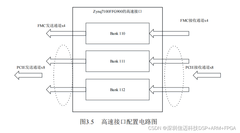
The XC7Z100FFG900 provides 16 GTX transceiver pairs in total. This design uses 12 of them: 4 pairs are routed to the FMC connector (bank 110) for the daughter-card optical link, and 8 pairs are routed to the PCIe edge connector (banks 111 and 112).
The high-speed interface block diagram is shown in Figure 3.5.
(5) Peripheral Configuration and Boot Circuit
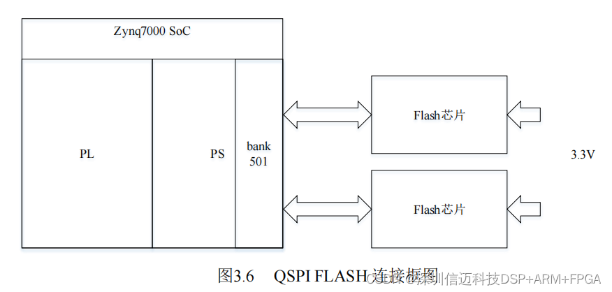
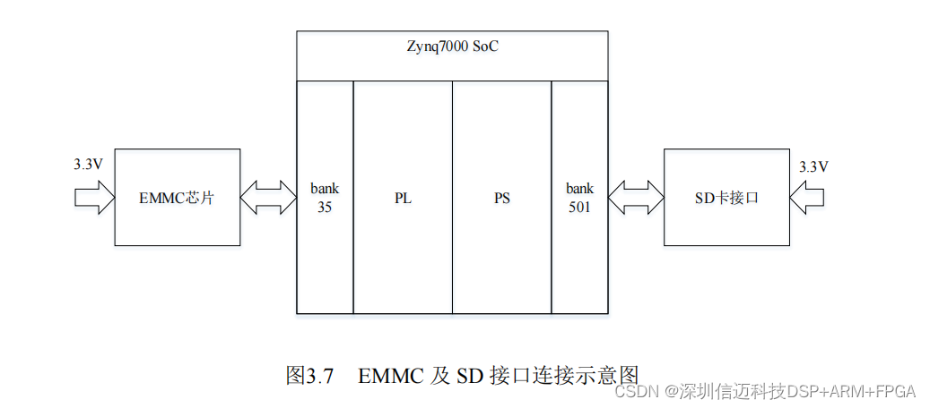
Like all Xilinx FPGAs and SoCs, the Zynq-7000 is volatile: the PL bitstream and PS software are lost when power is removed. The design therefore provides multiple non-volatile storage options:
- Two QSPI Flash chips — Cypress S25FL256S, 256 Mb each, connected to PS bank 500. Maximum read/write clock is 133 MHz.
- One SD card interface — connected to PS bank 501, used for storing the boot image or OS.
- One eMMC device — Micron MTFC8GAKAJCN-4M, 8 GB capacity, 50 MHz clock, connected to PL bank 35 and accessed via the EMIO feature.
The QSPI Flash connection block diagram is shown in Figure 3.6, and the eMMC / SD card connection diagram is shown in Figure 3.7.
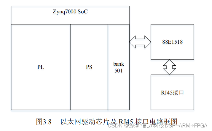
For remote control and firmware updates over the network, a standard RJ-45 Gigabit Ethernet port is provided. The PHY is the Marvell 88E1518, a tri-speed (10/100/1000 Mbps) Ethernet transceiver connected to PS bank 501. The network port and PHY block diagram is shown in Figure 3.8.
3.2.2 DDR3 SDRAM Selection and Configuration
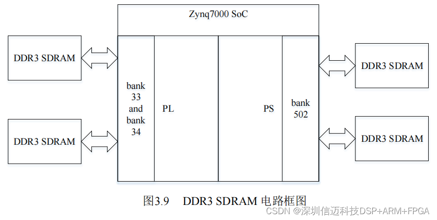
Both the PS and PL domains require external DDR3 SDRAM. The PS-side DRAM provides a working memory region during boot and OS operation, while the PL-side DRAM serves as the high-bandwidth data cache for buffering incoming high-speed acquisition data before it is transferred to the host over PCIe.
The design uses Micron MT41K256M16TW-107 DDR3 SDRAM. Two chips are populated on each of the PS and PL sides, giving a 32-bit data bus width per domain (2 × 16-bit devices) and a total capacity of 1 GB per domain. Key performance figures:
- PS-side DDR3: up to 1066 MHz operating frequency.
- PL-side DDR3: up to 1600 MHz operating frequency.
The PL-side DDR3 is connected to HP banks 33 and 34, which offer cleaner power rails and tighter I/O timing margins compared to HR banks — important for extracting maximum DDR3 performance. The PS-side DDR3 connects to the dedicated memory interface bank 502. The DDR3 block diagrams for both domains are shown in Figure 3.9.
3.2.3 High-Speed Interface Circuit
The carrier board provides two classes of high-speed interfaces: FMC and PCIe.
As a general PCB layout rule, 0.1 µF AC-coupling capacitors are placed at every high-speed differential signal pin to block DC offsets. Differential pairs within a single channel are routed as tightly coupled, parallel traces on the same layer to minimize impedance discontinuities, and vias between layers are kept to a minimum. Across multiple channels, all differential pairs are length-matched to ensure phase-aligned, synchronous data reception.
FMC (FPGA Mezzanine Card) is the VITA 57.1 standard interconnect between a carrier board and a daughter card. The daughter card typically carries the male connector and the carrier board the female connector. FMC supports transfer rates up to 10 Gbps per lane, with a theoretical aggregate throughput approaching 40 Gbps. Two variants exist:
- LPC (Low Pin Count): 160-pin connector.
- HPC (High Pin Count): 400-pin connector, used here because it provides the required number of GTX transceiver lanes.
In addition to the high-speed data lanes, the FMC connector also carries a JTAG chain, an I²C management bus, and dedicated power pins that allow the carrier board to supply the daughter card directly. This decouples the daughter-card logic design from the carrier board's general-purpose FPGA I/O pin constraints and makes the daughter-card design more portable.
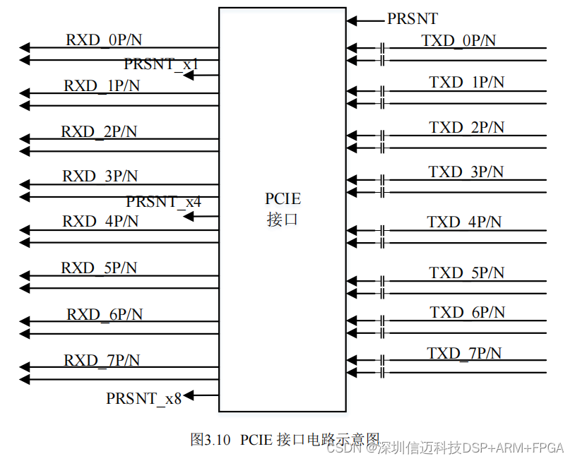
The PCIe interface (Figure 3.10) uses a gold-finger edge connector that plugs directly into a host PC motherboard slot. RXD pins receive data from the host; TXD pins transmit to the host. AC-coupling capacitors (0.1 µF) are required on the TXD differential lines. The PCIe lane width is selectable — X1, X2, or X8 — by connecting the appropriate PRSNT_xx pin to PCIE_PG. This design implements PCIe X8 mode, requiring PRSNT_x8 to be tied to PRSNT.
3.2.4 Power Circuit
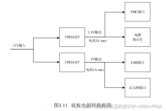
A well-designed power delivery network is critical: excessive output ripple causes instability, performance degradation, and can permanently damage components. The PC motherboard supplies the PCIe slot at 12 V, so the acquisition card's primary input is 12 V DC, which is then down-converted by on-board power management ICs to supply each subsystem at its required voltage.
Power management ICs must not be operated at or beyond their rated output current, since that leads to voltage droop and thermal runaway. The Zynq-7000 is a low-power SoC; its combined PS + PL current draw in this application is within a few amperes, which is well within the budget of the chosen regulators.
The design uses a core board + baseboard split. The main control chip sits on the core board. Performing all power conversion on the baseboard would complicate the baseboard layout and tightly couple the core board to a single baseboard design. Instead, the 12 V rail is brought onto the core board and converted there — making the core board self-contained and reusable with other baseboards.
The baseboard still needs modest power conversion for its own peripherals (USB, Ethernet PHY, FMC power delivery). That conversion is handled by a TI DC/DC converter with an input range of up to 18 V and a programmable output range up to 7 V, rated for up to 3 A output — sufficient for the baseboard's peripheral load. The baseboard power block diagram is shown in Figure 3.11.
The core board requires multiple supply voltages — 0.75 V, 1.0 V, 1.5 V, 1.8 V, 2.0 V, 3.3 V, and 5.0 V — for the Zynq SoC, DDR3 SDRAM termination and core, and other peripherals. The full core-board power conversion tree is shown in Figure 3.12.
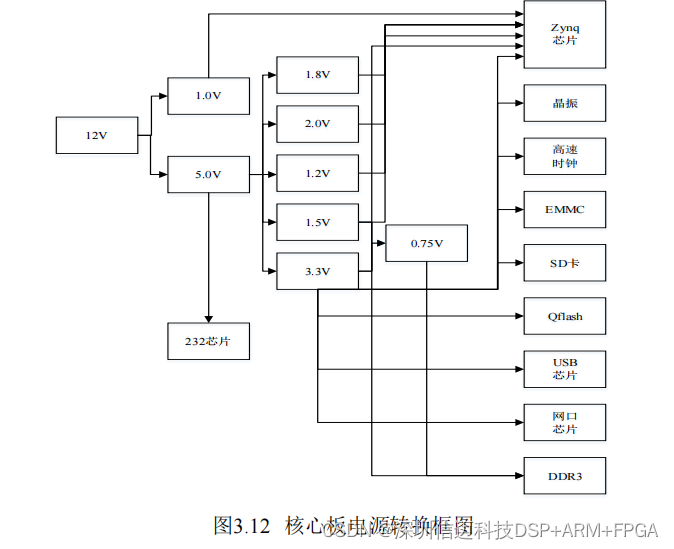
Key power IC choices on the core board:
- 12 V → 1 V (Zynq PL core): TI TPS53355. Conversion input range 1.5–15 V; bias supply input range 4.5–25 V; adjustable output down to a fraction of a volt; maximum output current 30 A.
- 12 V → intermediate rail: TI DC/DC converter with 6 A output capability and output adjustable from 0.76 V upward.
- 5 V → lower voltages (1.5 V, 1.8 V, etc.): MPS MP2143, input range 2.5–5.5 V, output range 0.6 V to Vin − 0.5 V, 3 A output capability.
All selected ICs were verified to meet the actual load current demands with margin, ensuring stable operation across the full operating range.
3.3 Daughter Card Circuit Design
3.3.1 AD Daughter Card Circuit Design
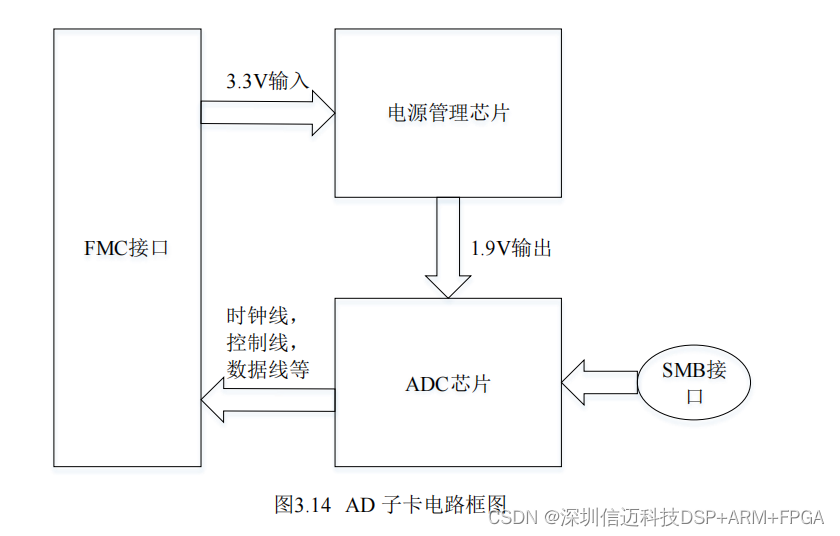
The ADC daughter card performs analog-to-digital conversion of the incoming radar IF/baseband signal and delivers the digitized samples to the Zynq chip over the FMC interface.
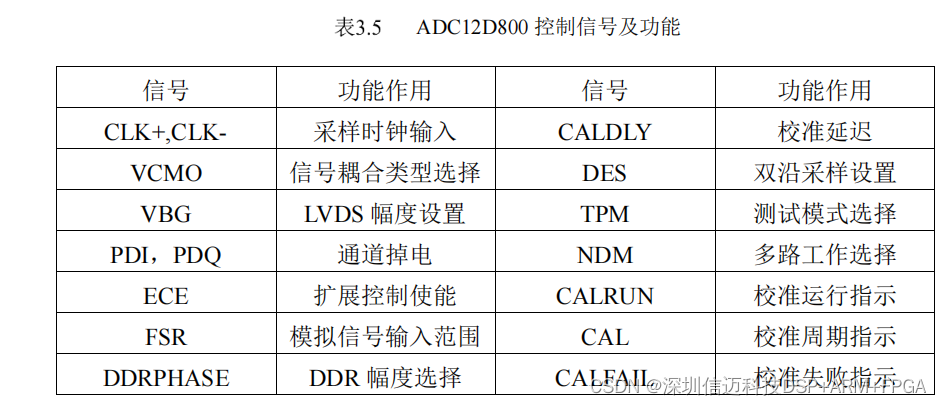
The ADC is the TI ADC12D800, a dual-channel, 12-bit converter with a maximum sample rate of 1.6 GSPS (interleaved). Its output can be configured either as 12 differential output pairs or as parallel data lines. The two independent channels are designated I and Q, each with its own dedicated data bus, supporting both single-edge (SDR) and double-edge (DDR) clocking modes. The ADC's clock and control interface signals are summarized in Table 3.5.
The ADC12D800 also provides an SPI interface for extended control mode, enabling software configuration of offset trim, calibration, and other parameters. This design does not use the SPI configuration path, so that interface is not discussed further here.
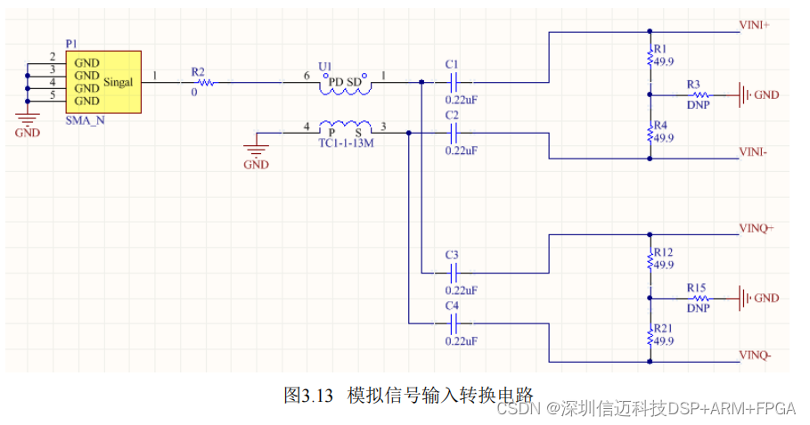
The analog input is AC-coupled — the incoming RF/IF signal enters through an SMB coaxial connector, passes through the matching and balun network, and is converted to a differential signal pair before entering the ADC's differential input pins. The input circuit is shown in Figure 3.13.
The ADC12D800's maximum operating voltage is 2.2 V. This design powers it at 1.9 V, derived from the 3.3 V supply available on the FMC connector using a TI LP38503-ADJ LDO regulator (input range 2.7 V to 6 V, output range adjustable up to 5.0 V, maximum output current sufficient for the ADC load).
All ADC control lines and data lines are brought out to the FMC connector, with equal-length routing enforced on the data bus to satisfy timing closure for synchronous parallel capture. The complete AD daughter card block diagram is shown in Figure 3.14.
3.3.2 Fiber-Optic Daughter Card Circuit Design
The fiber-optic daughter card provides the physical-layer bridge between the optical fiber link and the FMC connector on the carrier board. Its primary component is a QSFP (Quad Small Form-factor Pluggable) connector (part number 1761987-9), which exposes 4 high-speed differential transceiver lanes in a compact, hot-pluggable package well-suited for multi-lane fiber-optic links.
The optical transceiver module used is an SR4-40G QSFP+ module, offering an aggregate line rate of 40 Gbps (4 × 10 Gbps) over multi-mode fiber with a reach of up to 150 m. The QSFP cage requires a 3.3 V supply, which is drawn directly from the FMC power pins provided by the carrier board. The four high-speed differential pairs from the QSFP connector are routed directly to the FMC HPC connector, where they connect to the GTX transceiver lanes in bank 110 of the Zynq-7100.
This passthrough architecture keeps the fiber daughter card simple: it performs no signal conditioning beyond the optical-to-electrical conversion inside the QSFP module, and the Aurora protocol framing and 8b/10b encoding are handled entirely within the Zynq PL fabric. Equal-length routing and controlled-impedance traces are used on the high-speed differential lines between the QSFP cage and the FMC connector to preserve signal integrity at 10 Gbps per lane.
Summary
The hardware design presented in this chapter covers every major subsystem of the Zynq-based 10 Gbps PCIe acquisition card:
| Subsystem | Key Choice |
|---|---|
| Main control SoC | XC7Z100FFG900-2 (Zynq-7100, dual Cortex-A9 + Kintex-7 PL) |
| GTX transceivers used | 12 of 16 pairs (4 FMC / 8 PCIe) |
| PS DDR3 | 2 × Micron MT41K256M16TW-107, 32-bit / 1 GB, 1066 MHz |
| PL DDR3 | 2 × Micron MT41K256M16TW-107, 32-bit / 1 GB, 1600 MHz |
| GTX reference clock | TI CDCM61002, 62.5–625 MHz DIP-selectable |
| Non-volatile storage | 2 × Cypress S25FL256S QSPI Flash + SD card + 8 GB eMMC |
| Ethernet PHY | Marvell 88E1518 (10/100/1000 Mbps) |
| ADC daughter card | TI ADC12D800, 12-bit, 1.6 GSPS, dual I/Q channels |
| Fiber daughter card | QSFP SR4-40G, 40 Gbps aggregate over 150 m MMF |
| Primary power input | 12 V DC (from PCIe slot), down-converted on core board |
The carrier-board / daughter-card split via the FMC HPC connector gives this platform its modularity: the same Zynq carrier can be paired with different signal-conditioning daughter cards (ADC, fiber, DA, etc.) simply by swapping the mezzanine module, while the Zynq PL firmware adapts to the new interface. This approach is characteristic of the VITA 57.1 ecosystem and substantially reduces the NRE cost of iterating on front-end hardware.