[Domestic Virtual Instruments] Design of a Dual-Channel 6.4GSPS High-Speed Data Acquisition Module Based on FPGA+JESD204B Clock (Part 2) Research on JESD204B Link Establishment and Synchronization Process
Design of Acquisition and Data Reception Circuit Based on JESD204B
This article is Part 2 of a series on building a dual-channel 6.4 GSPS high-speed data acquisition module using FPGA and JESD204B. Here we focus on the JESD204B protocol internals: how the interface is structured, how a link is established from scratch, and how multi-device synchronization is achieved using deterministic latency under Subclass 1. Engineers integrating high-speed ADCs such as the TI ADC12DJ3200 into FPGA-based acquisition systems will find the link bring-up sequence and SYSREF calibration procedure especially practical.
3.1 JESD204B Protocol Overview
To address the ever-increasing data throughput demands of high-sampling-rate, high-resolution data converters, the JEDEC association developed JESD204 — a high-speed serial communication protocol bridging data converters and logic devices — and has released successive revisions since. The second revision, JESD204B, has been widely adopted by leading device vendors including Analog Devices (ADI) and Texas Instruments (TI) for their high-speed converter product families.
Compared to its two predecessors, JESD204B introduced three key advances:
- Higher lane rate — the maximum single-lane data rate increased to 12.5 Gbps.
- Device clocking model — transmitter and receiver no longer share a common frame clock. Instead each device uses its own device clock (the converter's sampling clock on the ADC side; a reference clock on the FPGA side). These two clocks typically run at different frequencies.
- Deterministic latency — repeatable, programmable per-lane delay solves the multi-lane, multi-channel alignment problem across power cycles and link re-establishments.
Based on deterministic-latency support and the clock mechanism used to implement it, JESD204B is divided into three subclasses:
| Subclass | Deterministic Latency | Clock Reference |
|---|---|---|
| 0 | No | Frame clock |
| 1 | Yes | SYSREF + LMFC |
| 2 | Yes | SYSREF + LMFC (AC-coupled variant) |
Only Subclasses 1 and 2 guarantee repeatable latency across power cycles, making them the correct choice for multi-device synchronous acquisition.
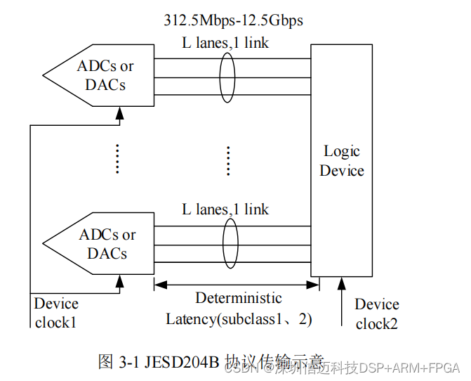
3.2 JESD204B Interface Structure
A JESD204B interface consists of a transmitter (typically the ADC or DAC) and a receiver (typically the FPGA logic device). Both sides share the same four-layer architecture:
- Application layer — not formally defined by the JESD204B standard, but conventionally refers to the user-accessible interface for configuring link parameters. Both sides must be programmed with identical parameters for the link to function.
- Transport layer — maps converter sample data into bytes, frames, multi-frames, and lanes according to the link parameters L, M, F, S, CS, N, and N′. On the receive side, the transport layer reconstructs the original samples from the packed lane data.
- Data link layer — responsible for link establishment, synchronization, and monitoring. Core functions include 8b/10b encoding/decoding, and the CGS/ILS synchronization sequences described below.
- Physical layer — serializes encoded data for transmission and deserializes received serial data. Physically implemented with CML-level drivers, pre-emphasis (transmit side), equalizers (receive side), and a clock-data recovery (CDR) module.
The key link parameters appearing in the transport layer are:
- L — number of lanes per link
- M — number of converters per device
- F — number of octets per frame per lane
- S — number of samples per frame clock per converter
- N — converter resolution (bits)
- N′ — total bits per sample including control and tail bits
- CS — number of control bits per sample
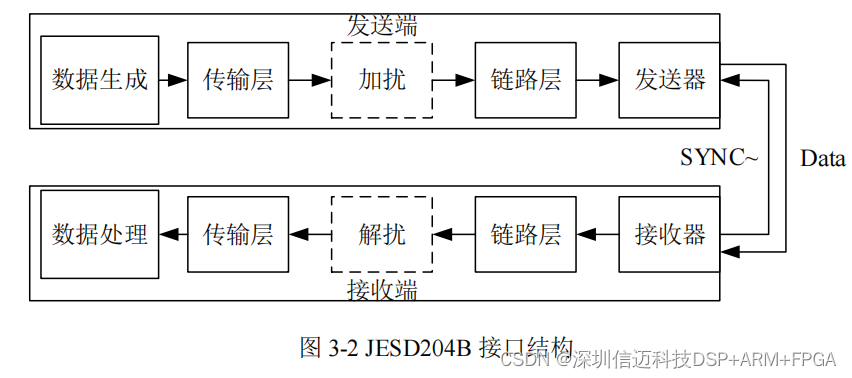
8b/10b encoding at the link layer deserves particular attention. It guarantees DC balance on AC-coupled serial links by preventing runs of six or more identical bits, ensuring sufficient edge transitions for CDR lock at the receiver. It also provides basic error detection: any received 10-bit character absent from the decoder lookup table indicates a bit error in that character.
An optional scrambler sits between the transport and link layers on the transmit side. When enabled, it eliminates spectral spurs that could arise from repetitive data patterns; the receiver must apply the corresponding descrambler after 8b/10b decoding.
3.3 JESD204B Link Establishment and Synchronization
Link bring-up proceeds in two mandatory phases before user data flows: Code Group Synchronization (CGS) and Initial Lane Synchronization (ILS). Initial Frame Synchronization (IFS) is embedded within both phases.
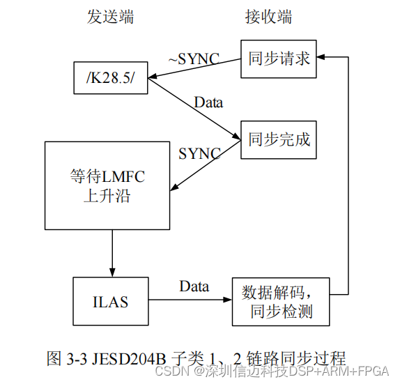
Phase 1 — Code Group Synchronization (CGS)
CGS aligns the receiver's byte clock to the character boundaries in the incoming serial stream.
- The receiver pulls SYNC low, signaling a sync request to the transmitter.
- The transmitter responds by continuously sending the K28.5 character (
0xBCin hex), also written as/K/. - The receiver scans the incoming stream for at least four consecutive valid K28.5 characters. When found, it pulls SYNC high to release the sync request.
- The transmitter continues sending K28.5 until the next LMFC (Local Multi-Frame Clock) boundary, at which point CGS is complete.
For Subclass 1, the SYSREF signal must have already been used to align the frame clock and multi-frame clock boundaries across all devices before CGS begins.
Phase 2 — Initial Lane Synchronization (ILS)
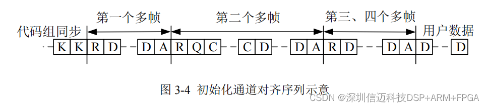
ILS detects frame and multi-frame boundaries in the lane data stream and verifies that the receiver's link parameters match what the transmitter was programmed with. It is carried out via the Initial Lane Alignment Sequence (ILAS).
For Subclasses 1 and 2, ILAS consists of exactly 4 multi-frames. Each multi-frame is structured as follows:
- Starts with /K28.0 (
0x1C, the/R/character — Frame Start) - Ends with /K28.3 (
0x7C, the/A/character — Lane Alignment) - The second multi-frame additionally contains /K28.4 (
0x9C, the/Q/character — Link Configuration Start) immediately after the start character, followed by the actual link parameter values (character C). Unfilled positions in the ILAS are padded with ramp data (character D).
During user data transmission, frame alignment errors may occur. They are corrected by inserting or replacing specific frame positions with the alignment characters /K28.7 (0xFC, /F/) and /K28.3, then verifying the alignment character positions at the receiver.
3.4 Multi-Device Synchronization Based on JESD204B
In a multi-channel acquisition system, synchronization means that multiple ADC devices sample simultaneously, transmit their data in phase with each other, and maintain a stable and repeatable inter-channel phase relationship across power cycles. Achieving this over JESD204B requires two things: (1) phase-aligned sampling clocks across all ADCs, and (2) synchronous data transport.
Beyond the physical trace-length matching used in LVDS parallel interfaces, JESD204B provides two software-level synchronization mechanisms: time-stamping and deterministic latency. In practice, deterministic latency (implemented via Subclasses 1 or 2) is the predominant approach.
3.4.1 Deterministic Latency
The JESD204B standard formally defines deterministic latency as the time difference between a sample entering the serial transmitter in frame structure and the same sample exiting the serial receiver in frame structure.
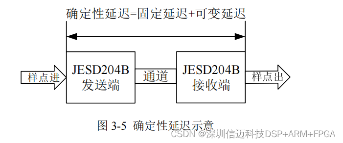
Total latency = fixed delay + variable delay. The variable component arises because the phase relationships among the multiple clocks involved in data transmission and processing are non-deterministic at each power-up or link re-establishment.
Subclass 0 can align multiple channels on a single link without external circuitry, but cannot fix the latency across power cycles — ruling it out for multi-link synchronous systems.
Subclasses 1 and 2 address this by requiring:
- The transmitter to begin sending ILAS on all lanes at the same "deterministic moment" — specifically, the LMFC boundary following SYNC deassertion (programmable to a configurable number of LMFC edges after SYNC rise).
- The receiver to release all buffered channel data simultaneously at a "deterministic moment" defined as a programmable number of frame periods after the next LMFC boundary — this value is called RBD (RX Buffer Delay), ranging from 1 to K.
To ensure all channel data has arrived before release, the maximum delay across all channels must be less than one local multi-frame period, and RBD × frame_period > max_channel_delay.
In the JESD204B IP core, register 0x030 holds the RBD value. Each lane also exposes a Buffer Adjust register indicating its receive buffer fill level. The minimum deterministic latency is achieved by reading all Buffer Adjust registers, finding the minimum value, and writing that value to RBD.
3.4.2 SYSREF Design
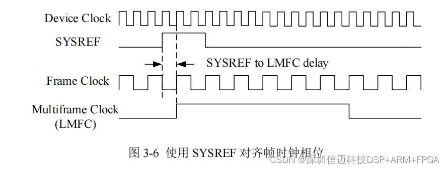
The deterministic transmit and receive release moments described above are both counted in units of the frame clock / multi-frame clock. Phase-aligning the frame and multi-frame clocks across all devices in the system is therefore the fundamental enabler of deterministic latency. Subclass 1 uses SYSREF to establish this common reference phase.
As converter sampling rates scale upward, meeting the SYSREF setup and hold window relative to the device clock becomes increasingly challenging. The ADC12DJ3200 used in this design operates at 6.4 GSPS. To widen the SYSREF setup/hold window, this ADC employs dual-edge sampling of the input clock in single-channel mode, effectively halving the required input clock frequency and doubling the SYSREF timing margin.
In addition to reduced input clock frequency, the ADC12DJ3200 provides two SYSREF management features:
- SYSREF Window — detects the SYSREF position relative to the device clock and helps the user select a sampling position that satisfies setup and hold requirements.
- SYSREF Auto-Calibration — easier to use than the window feature; adjusts the ADC aperture timing to shift the ADC sampling sequence relative to SYSREF, rather than requiring the user to adjust SYSREF phase manually.
SYSREF Window Procedure
- Apply the sampling clock and SYSREF to the ADC.
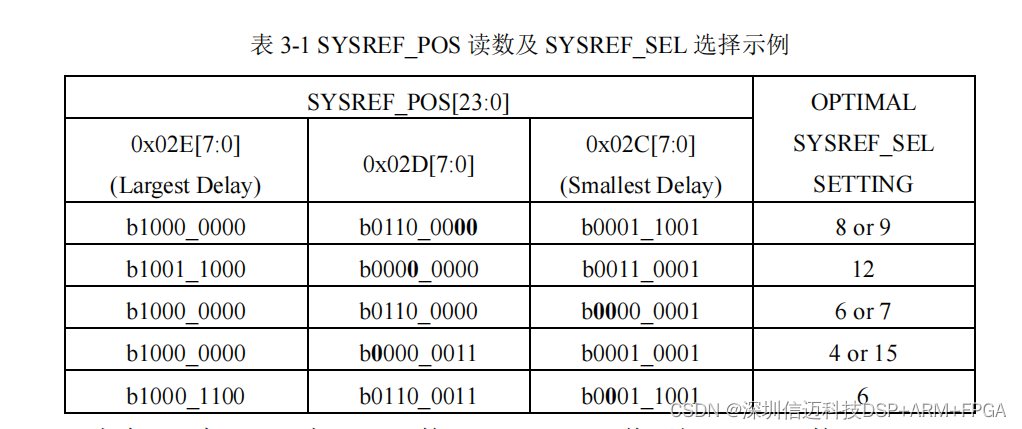
- The SYSREF capture block uses the SYSREF window to determine SYSREF's position relative to the device clock and stores it in the SYSREF_POS register. Each bit of SYSREF_POS represents one potential SYSREF sampling position; a set bit indicates a potential setup or hold violation at that position.
- Based on SYSREF_POS, write the SYSREF_SEL register to select the valid sampling position — typically the midpoint of the region where both setup and hold are satisfied. SYSREF_SEL supports values 0–15, covering the first 16 potential sampling positions.
- Adjust the sampling position step size using the SYSREF_ZOOM register. Set SYSREF_ZOOM = 0 when bits 0–23 of SYSREF_POS are all 1; otherwise set SYSREF_ZOOM = 1.
For this acquisition module, SYSREF_ZOOM was set to 1 and SYSREF auto-calibration was disabled before reading SYSREF_POS. The results for the two ADCs are shown in the table below:
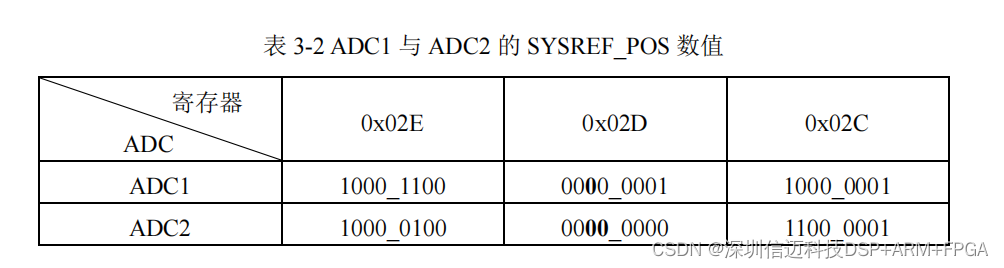
From the SYSREF_POS values, ADC1 requires SYSREF_SEL = 13 to satisfy setup and hold timing. ADC2 can use SYSREF_SEL = 12 or 13. Setting both ADCs to SYSREF_SEL = 13 satisfies timing on both devices simultaneously.
3.4.3 Multi-Device Synchronization via Deterministic Latency
The full Subclass 1 deterministic latency flow is as follows:
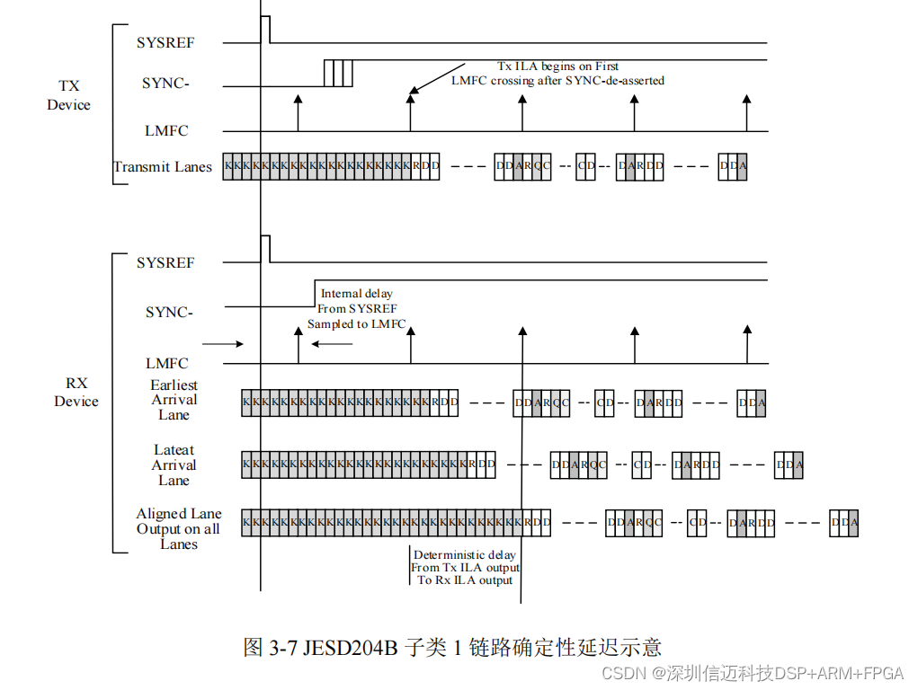
- SYSREF establishes the LMFC boundary on both transmitter and receiver sides.
- The transmitter begins link establishment when SYNC is pulled low.
- Each receiver channel's receive buffer accumulates valid data.
- Once valid data has arrived on all receiver channels, the buffers release all channels' data simultaneously at the next local LMFC boundary — at this point every data channel carries exactly one local multi-frame period of delay (RBD = K), and that delay is deterministic and repeatable.
Alternatively, buffered data may be released before the next LMFC boundary (RBD < K) — the minimum permissible RBD corresponds to the minimum deterministic latency.
One practical edge case to watch for: the maximum channel delay may not always fit within a single multi-frame period, and it is possible for two channels' valid data to arrive in adjacent LMFC windows rather than the same one. Both conditions require careful design of the LMFC period (K × F octets) relative to the maximum expected inter-channel skew.
Sienovo provides high-speed data acquisition solutions tailored for demanding FPGA-based instrument and industrial applications.