【Domestic Virtual Instrument】DSP+FPGA+ADS1282-based 32-Bit High-Precision Data Acquisition Solution (II) Analog Circuit Design
This article walks through the analog front-end and ADC circuit design for a 32-bit high-precision data acquisition system built around the TI ADS1282 delta-sigma ADC, an FPGA, and a DSP. Part II focuses on the signal-conditioning chain from sensor current output all the way to the FPGA's SPI interface, covering component selection rationale, filter design, ADC operating-mode selection, pin-level interfacing, SPI timing constraints, multi-channel synchronization, and register-level control.
System Architecture Overview
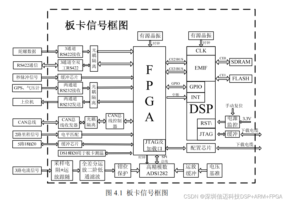
Figure 4.1 shows the hardware signal block diagram. The digital signal processing board centers on two processing chips: an FPGA and a DSP. The FPGA acts as the bridge between the DSP and all peripheral interfaces and handles data pre-processing, while the DSP is the computation core.
The FPGA receives data from external devices over various data buses, performs packetization and other pre-processing, and stores results in designated on-chip memory. The DSP reads this data via its EMIF bus interface and executes the data-solving algorithms. Intermediate parameters and final results are written by the DSP back into FPGA-internal memory via EMIF, after which the FPGA transmits them externally over the CAN bus interface.
4.2 High-Precision Data Acquisition Circuit Design
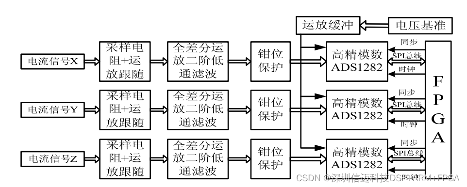
Figure 4.2 shows the structural block diagram of the data acquisition module. Because the sensors output current signals while the ADS1282 requires a differential voltage input, the first task is current-to-voltage conversion. A high-precision, low-temperature-coefficient sampling resistor performs this conversion. The resulting voltage then passes through a second-order low-pass filter built from a fully-differential op-amp, which removes high-frequency noise. The filtered signal goes through clamp protection diodes before entering the ADS1282's differential inputs. The clamp diodes protect the ADC against instantaneous input overload: when the input signal level exceeds the rating of the internal ESD diodes, the external clamp diodes engage and limit the voltage, preventing damage. The ADC's digital communication interface connects directly to the FPGA, which implements an SPI bus in fabric to read the converted data.
4.2.1 Analog Signal Conditioning Circuit Design
1. Current Sampling
Accelerometer signals demand very high precision, so front-end circuit topology and component selection are critical. The op-amp must exhibit high common-mode rejection ratio (CMRR), high precision, low drift, and low noise. The low-pass filter must have excellent linearity and a well-defined cutoff frequency, and the analog front end must accept differential input.
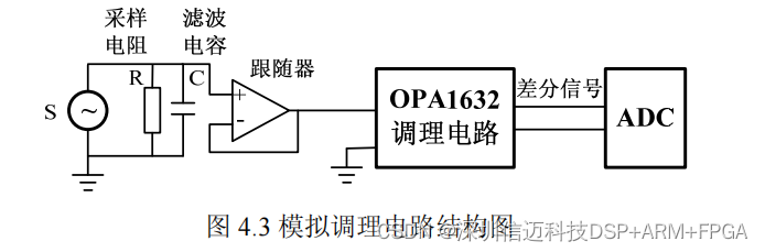
As shown in Figure 4.3, the input current signal passes through a sampling resistor to produce a proportional voltage. The stability and accuracy of that voltage depend directly on the resistor's performance. The design uses a VISHAY VSMP-series ultra-precision metal-foil resistor, chosen for its excellent load-life stability, near-zero temperature coefficient of resistance, extremely low noise, and tight resistance tolerance.
A filter capacitor C provides additional high-frequency attenuation at the resistor output. The resulting voltage is buffered by a voltage-follower op-amp before entering the conditioning stage. The buffer is an OPA227, selected for its combination of very low noise (3 nV/√Hz), wide bandwidth (8 MHz), very high CMRR (138 dB), high open-loop gain (160 dB), low output offset voltage (75 µV max), extremely low temperature drift (0.1 µV/°C), and wide supply voltage range (±2.5 V to ±18 V). It operates across −55 °C to +125 °C.
2. Conditioning Circuit
The ADS1282 uses a differential voltage input. Differential signaling's primary advantage is strong noise immunity: external interference couples onto both signal lines nearly simultaneously and is cancelled when the difference is taken. The two signal lines also cancel each other's radiated electromagnetic fields. Differential switching transitions occur at the signal crossing point, making timing less sensitive to process and temperature variation.
Because the ADC input is differential while the signal source is single-ended, a low-noise analog conditioning circuit is needed to interface them. There are two common single-ended-to-differential conversion approaches: (1) a multi-op-amp discrete circuit, and (2) a single fully-differential op-amp IC. The discrete approach inevitably introduces more noise sources. The single-chip approach is simpler and uses fewer components, so this design uses a single fully-differential op-amp — the OPA1632 — for the front-end analog signal conditioning and filtering function.
The OPA1632 is a high-performance, low-noise fully-differential op-amp with THD as low as 0.000022% and noise density as low as 1.3 nV/√Hz. The voltage from the sampling resistor, after capacitor filtering, feeds into the OPA1632.
As shown in Figure 4.4, the OPA1632 is configured as a second-order Butterworth low-pass filter. The passband width is set by selecting appropriate resistor and capacitor values to meet design requirements. The Butterworth topology is chosen because it provides maximally flat frequency response within the passband — no ripple — while attenuating monotonically outside the passband.
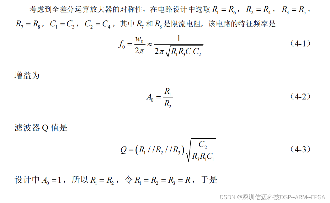
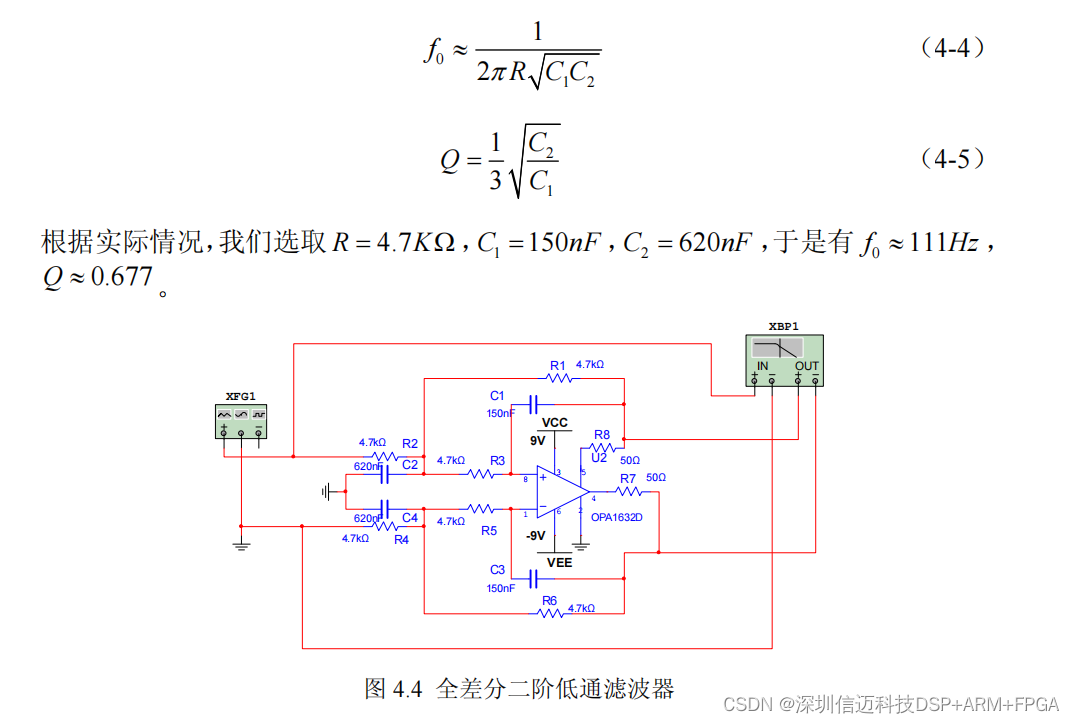
Figure 4.5 shows the Multisim-simulated Bode plot for this low-pass filter. The gain curve is very flat within the passband with no ripple, and attenuation outside the passband is rapid, confirming the filter performs as designed.
4.2.2 ADC Circuit Design
Operating Mode and SNR Selection
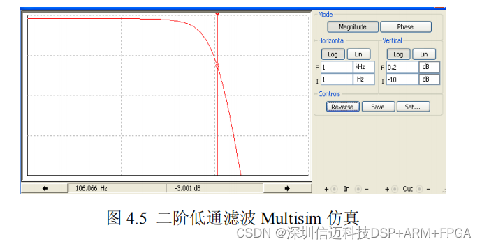
The ADS1282 supports two primary operating modes selectable via register: low-power mode and high-performance mode. SNR varies with mode, output data rate, and on-chip PGA gain setting. Under equal conditions, high-performance mode always yields better SNR than low-power mode. Lower data rates and lower PGA gain also improve SNR.
This design selects high-performance mode at 500 SPS. The SNR at this operating point is 127 dB. Using the standard ENOB formula, this corresponds to an effective number of bits of 20.8, which meets and exceeds the system's precision requirement.
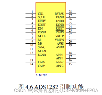
Pin Description
The ADS1282 is housed in a 28-pin TSOP SMD package. Key pin functions are as follows:
- CLK: Master clock input
- SCLK: Serial clock input
- **DRDY**: Data-ready output; data is read on its falling edge
- DOUT / DIN: Serial data output / input
- MCLK, M1, M0: In modulator-output mode, MCLK is the modulator clock output and M1/M0 are modulator data outputs; otherwise these pins must be tied to fixed levels
- SYNC: Synchronization input for multi-chip synchronized operation
- MFLAG: Over-range flag; logic 0 = normal, logic 1 = over-range
- DGND: Digital ground reference
- CAPP / CAPN: Internal PGA output pins; a 10 nF capacitor must be connected between them
- AINP2 / AINN2, AINP1 / AINN1: Positive/negative analog inputs for channels 2 and 1
- AVDD / AVSS: Analog supply; single-ended +5 V or bipolar ±2.5 V
- VREFP / VREFN: Positive/negative reference voltage inputs
- **PWDN**: Power-down input, active low
- **RESET**: Reset input, active low
- DVDD: Digital supply, +1.8 V to +3.3 V
- BYPAS: Calibration output; requires a 1 µF capacitor to DGND
1. ADC Internal Architecture and Operating Principle
The ADS1282's internal structure (Figure 4.7) consists of a multiplexer (MUX), a programmable gain amplifier (PGA), a fourth-order delta-sigma (Δ-Σ) modulator, a programmable digital filter, an over-range detection circuit, gain and offset calibration modules, a controller, and an SPI serial bus interface.
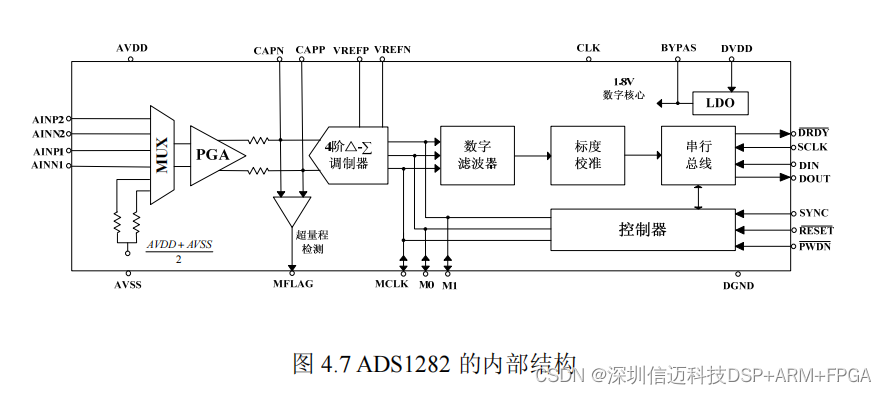
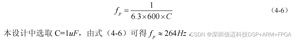
The MUX supports five configurations: channel 1 input, channel 2 input, short-circuit between the two channel inputs of the same polarity, an internal 400 Ω short-circuit test, and a common-mode test. Following the MUX is the differential-input, differential-output PGA with a gain range of 1 to 64, configured via the PGA[2:0] bits of the CONFIG1 register. The PGA drives the modulator differentially through internal 300 Ω resistors. A COG-type ceramic capacitor connected between CAPP and CAPN serves as an anti-aliasing filter, eliminating instantaneous interference generated during modulator sampling. Its corner frequency is determined by this capacitor value and the internal resistance.
The ADS1282 modulator is a high-performance, inherently stable fourth-order Σ-Δ modulator. It pushes quantization noise to frequencies well above the signal band, where the digital filter can remove it effectively. The modulator differential input signal VIN = (AINP − AINN) × PGA has a range equal to VREF = VREFP − VREFN, i.e., ±2.5 V. When the modulator input exceeds full-scale, the modulator enters a stable saturation state, the digital output code locks to the positive or negative full-scale value, and the MFLAG pin transitions from low to high, providing a hardware over-range indicator. The modulator sampling frequency is CLK/4 = 1.024 MHz in high-performance mode and CLK/8 = 512 kHz in low-power mode, where the master clock CLK is 4.096 MHz.
The modulator's bitstream output can be accessed directly or routed through the on-chip digital filter. Setting FILTR[1:0] = 00 in the CONFIG0 register puts the modulator into output mode, where M0 and M1 become modulator data outputs and MCLK becomes the modulator clock output. When not in output mode, these pins are inputs and must be tied to fixed levels.
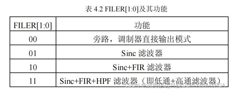
As shown in Figure 4.8, the digital filter receives and decimates the modulator bitstream. It consists of three cascaded stages: a five-stage sinc filter with adjustable decimation ratio, a 32× decimation finite impulse response (FIR) low-pass filter with programmable phase, and a programmable first-order high-pass filter (HPF). Data can be tapped after any stage. If no on-chip filtering is desired, the raw modulator output is available. This design uses the sinc filter plus the FIR low-pass filter path with the 500 SPS filter configuration.
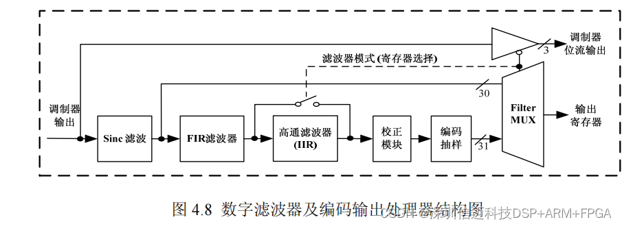
The digital filter output path is selected via the FILTR[1:0] bits as summarized in Table 4.2.
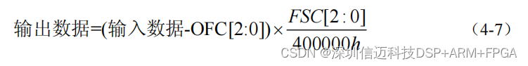
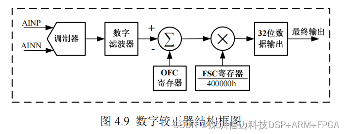
After the on-chip filter stages, a digital correction module consisting of an adder and a multiplier (Figure 4.9) applies offset and gain correction to the raw data according to the values stored in the OFC (offset calibration) and FSC (full-scale calibration) registers.
2. ADC Data Output Interface Circuit
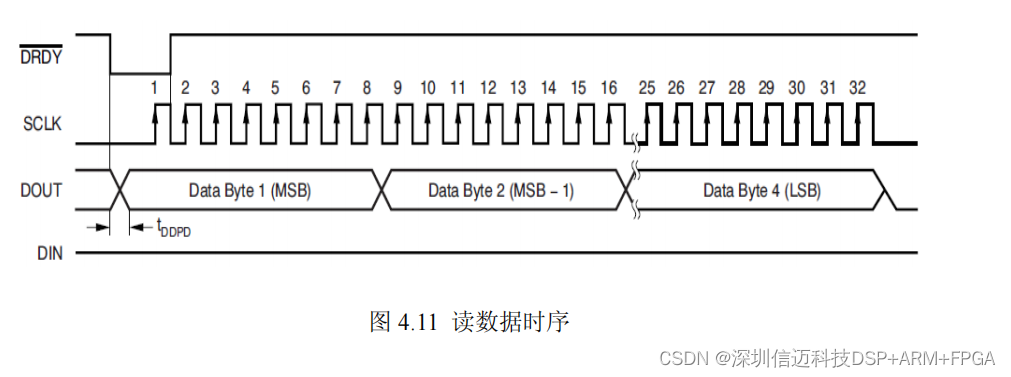
The ADS1282 communicates via SPI. Conversion data is output as 32-bit two's-complement values, MSB first, with the MSB serving as the sign bit (0 = positive, 1 = negative). The SPI interface uses three core signals: SCLK, DIN, and DOUT. Data is clocked into DIN on the rising edge of SCLK and shifted out of DOUT on the falling edge. When DRDY\ goes low, a new conversion result is ready and the FPGA can initiate a read. If SCLK remains low for 64 consecutive DRDY\ periods, any ongoing data transfer or command is aborted and the SPI interface resets; the next SCLK pulse starts a new communication cycle. SCLK must be held low when idle.
Figure 4.10 shows the SPI timing requirements:
- t_SCLK: SCLK period — minimum 2/f_sclk, maximum 16/f_sclk
- t_SPWHL: SCLK pulse width — minimum 0.8/f_sclk, maximum 10/f_sclk
- t_DIST: DIN setup time — minimum 50 ns
- t_DIHD: DIN hold time — minimum 50 ns
- t_DOPD: Delay from SCLK falling edge to new DOUT valid — maximum 100 ns
- t_DOHD: Hold time from SCLK falling edge to DOUT change — minimum 0 ns
- t_SCD_L: Interval from last rising edge of a command to first rising edge of a register read/write — minimum 24/f_sclk
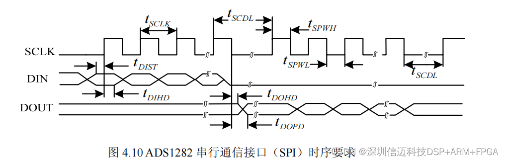
Figure 4.11 shows the SPI read-data timing. Each data packet is four 8-bit bytes (32 bits total), transmitted MSB first out of the DOUT pin.
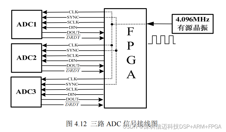
Multi-Channel Synchronization
This system uses three ADS1282 channels that must operate synchronously to avoid inter-channel timing errors. Synchronization can be achieved either through the SYNC pin or by issuing a sync command over SPI. When a sync event occurs, the ADC resets its internal memory and begins a new conversion. The ADS1282 supports two sync modes:
(1) Single-pulse sync mode. The ADC synchronizes only once during operation. Synchronization occurs at the first CLK rising edge after the SYNC rising edge, or at the eighth SCLK rising edge after a sync command. After this single sync event, the ADC continues converting at the selected rate without further synchronization.
(2) Continuous sync mode. The ADC re-synchronizes on every SYNC rising edge, performing one conversion per sync pulse.
This design uses SYNC-pin single-pulse synchronization. After all three ADC channels synchronize via the shared SYNC pin, they continue converting at the same rate continuously. Figure 4.12 shows the wiring of the three-channel ADC array. Each ADC's interface carries CLK, SYNC, SCLK, DIN, DOUT, and DRDY. Importantly, CLK and SYNC originate from the same internal FPGA signal, ensuring tight, deterministic synchronization across all three channels.
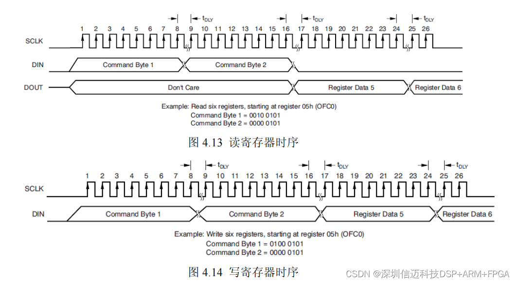
Register Access Protocol
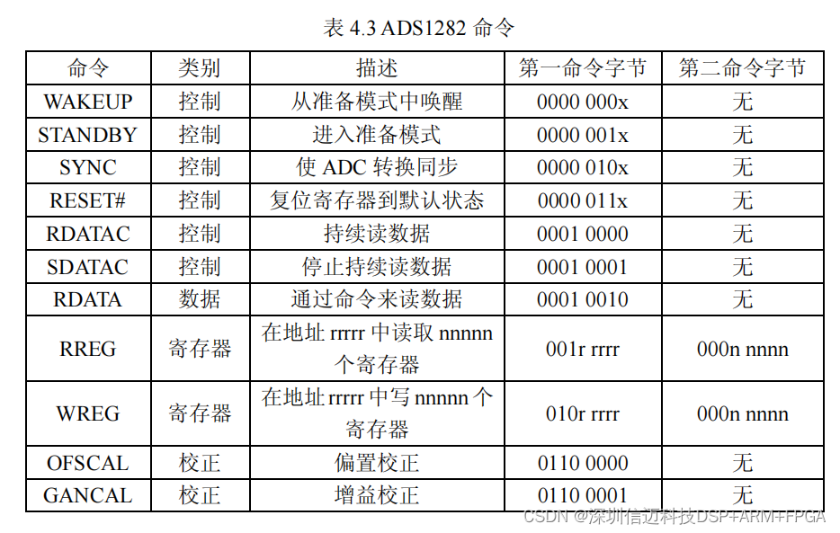
All ADS1282 control is exercised by sending commands over SPI, including register read and write operations. Figures 4.13 and 4.14 show the read and write register timing diagrams. A command word must be sent first; it encodes the starting register address and the number of registers to access (Table 4.3). The register data transfer follows immediately after the command word is clocked in.
4.2.3 Voltage Reference Design
A stable, low-noise voltage reference is essential for achieving the full dynamic range of a 32-bit ADC. The reference voltage VREF = VREFP − VREFN defines the modulator's input span of ±2.5 V, so any noise or drift on the reference directly adds to the ADC's output noise floor and degrades accuracy. The reference circuit design — covered in the next section — must match the precision of the sampling resistor, the OPA1632 conditioning stage, and the ADS1282 itself to avoid becoming the system bottleneck.