Domestic Virtual Instruments: Zynq-based Radar 10Gbps High-Speed PCIe Data Acquisition Card Solution (Part 1) Overall Design
Introduction
This article details the overall architecture of a Zynq-based high-speed PCIe data acquisition card designed for a radar emitter identification project. The card must capture, buffer, and transfer radar intermediate-frequency (IF) signals at sustained throughputs exceeding 19.2 Gbps — a requirement that drives every major design decision from ADC selection through PCIe lane count. The design uses a Xilinx Zynq7000 SoC as its central processor, combining an FPGA fabric (PL) with dual ARM Cortex-A9 cores (PS) on a single chip, and connects to an off-card recognition platform over a PCIe 2.0 x8 link.
2.1 Introduction
This project originates from a radar emitter identification initiative that requires acquisition, transmission, and storage of radar emitter intermediate-frequency (IF) signals. Based on those project requirements, this chapter introduces the overall design solution for the data acquisition card, covering both hardware and software. The chapter begins with a specification analysis, then presents the overall hardware architecture, then the software stack, and finally reviews the key protocols and technologies that make the system work.
2.2 Overall Design Overview
2.2.1 Acquisition System Specification Analysis
The radar emitter IF band in this project spans 760 MHz to 1060 MHz, making it a classic bandpass signal rather than a baseband signal. Treating it as a bandpass signal allows the bandpass sampling theorem to be applied: instead of sampling at twice the highest frequency (which would demand a rate well above 2 Gsps), only the occupied bandwidth matters for the Nyquist criterion. Applying the bandpass sampling formula yields a minimum theoretical sampling rate of 706.6 Msps.
In practice, real filters have transition bands and finite roll-off, so sampling exactly at the theoretical minimum causes spectral aliasing and unacceptable signal distortion. To provide margin, the AD daughter card in this design is specified at a maximum sampling rate of 1.6 Gsps with 12-bit resolution, giving a raw data rate of up to 19.2 Gbps — comfortably above the theoretical floor while leaving headroom for filtering guard bands.
The high-speed data stream produced by the ADC must cross several interface boundaries before reaching the host PC. Each boundary presents a potential bottleneck or clock-domain mismatch. Two architectural choices address this:
DDR3 SDRAM buffering. Direct connection between interfaces running at different clocks and widths risks data loss. DDR3 SDRAM resolves this by acting as an elastic buffer. DDR3 transfers data on both edges of the clock; at 800 MHz operation with a 16-bit bus, a single DDR3 device achieves a theoretical peak of 25.6 Gbps. To keep the board compact while still meeting throughput and capacity requirements, the design places two 16-bit DDR3 SDRAM devices on each of the PL and PS sides, forming 32-bit-wide buffers on both domains.
PCIe 2.0 x8 host interface. The host-facing interface must sustain at least 19.2 Gbps. PCIe 2.0 provides 5.0 Gbps per lane; running in x8 mode delivers a raw bandwidth of 40 Gbps — more than double the minimum requirement — ensuring the link is never the bottleneck.
2.2.2 Hardware Overall Design
The hardware follows a carrier card + daughter card topology connected via an FMC (FPGA Mezzanine Card) interface. FMC is an industry standard (VITA 57) that supports high-pin-count (HPC) and low-pin-count (LPC) variants with differential signal pairs capable of multi-Gbps rates per lane, making it well suited for interchangeable high-speed daughter cards.
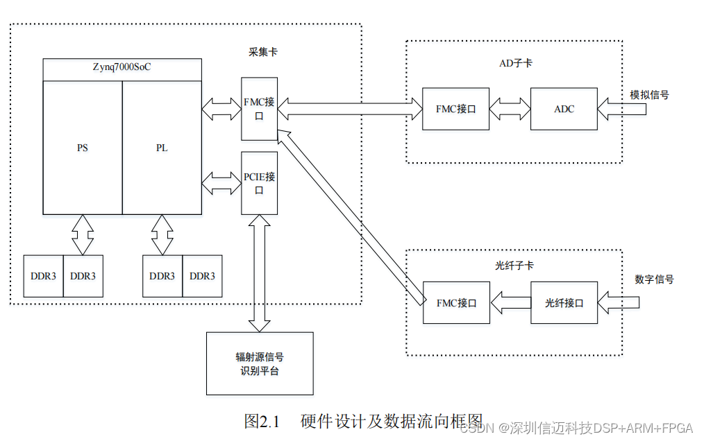
The carrier card is itself divided into a core board (the Zynq7000 SoC minimum system, with all chip I/Os broken out via connectors) and a base board (power delivery and peripheral interface routing). This split keeps the SoC layout clean and allows the base board to be revised without re-spinning the core.
Two interchangeable daughter card types provide acquisition flexibility:
- Optical fiber daughter card — receives high-speed digital signals already in the digital domain over multi-Gbps fiber links.
- AD daughter card — performs analog-to-digital conversion of the raw radar IF signal.
The AD daughter card uses an SMB RF connector for the analog input and is built around the TI ADC12D800, a dual-channel, 12-bit ADC supporting up to 1.6 Gsps maximum sample rate. Post-conversion data is output as 12 parallel LVDS differential pairs, supporting double-edge (DDR) clocking. All ADC signal lines are routed to the FMC connector for seamless integration with the carrier card. The optical fiber daughter card similarly routes its high-speed serial signals to FMC.
Data flow: daughter card → FMC → Zynq PL → DDR3 buffer (PL side) → PCIe 2.0 x8 → host PC recognition platform.
2.2.3 Software Overall Design
The software stack has three layers:
(1) FPGA Logic Design
Logic development targets Vivado 2017.4, Xilinx's integrated design environment for 7-series and Zynq devices. The design methodology is top-down and module-based, with five principal modules:
| Module | Function |
|---|---|
| Clock & Reset | Distributes clock and reset signals to all other modules |
| DDR3 SDRAM | High-speed data buffering using Xilinx MIG IP |
| PCIe | Data exchange with the host PC via PCIe 2.0 x8 |
| Aurora | Fiber-optic data receive and forward |
| ADC | ADC chip configuration, data capture, and forwarding |
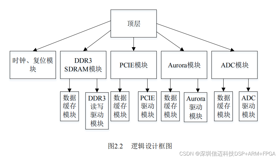
A critical design choice is the use of asynchronous FIFOs at every inter-module boundary. Because Aurora, PCIe, and the ADC interface each run on independent clock domains that cannot be easily synchronized, direct connections would cause metastability and data loss. Async FIFOs decouple read and write clocks entirely and allow the bus widths between modules to differ by integer multiples, giving the design flexibility to match each protocol's natural data width.
The fiber link uses 4 Aurora channels at 10 Gbps each (40 Gbps total), matching the PCIe 2.0 x8 link's 40 Gbps raw bandwidth. The FMC interface supports up to 10 Gbps per channel, which is why four channels are required to meet the 40 Gbps system throughput.
Vivado's IP catalog provides production-ready IP cores for PCIe, DDR3 MIG (Memory Interface Generator), and Aurora, avoiding the need to implement these complex protocols from scratch.
(2) Embedded Software Design
The ARM PS cores run Linux, developed using Vivado's bundled SDK environment on an Ubuntu host. The bring-up flow involves running a series of scripts to: compile the kernel, generate the device tree and FSBL (First Stage Boot Loader), build a root filesystem image, and write the combined boot image to the Zynq's SD card or flash. The embedded software layer is primarily a foundation for future user-space applications running on the PS side.
(3) Host PC (Upper Computer) Software Design
The host-side application runs on Windows and is responsible for:
- PCIe device open, close, and initialization
- DMA transfer length configuration
- Data reception and file storage for downstream processing
PCIe driver development uses WinDriver from Jungo Connectivity. WinDriver provides a kernel module (windrvr.sys) that handles the low-level OS kernel interactions, exposing a user-space function library so the application developer never needs to write kernel-mode code directly. This substantially reduces development risk and time compared to writing a WDM or WDF driver from scratch.
The application itself is built in Visual Studio. Because different host CPUs have different interrupt latency and throughput characteristics, the design uses DMA rather than programmed I/O (PIO) for all bulk data movement. The DMA transfer length is configurable from the host application rather than being hardcoded in the FPGA logic, giving the operator a tuning knob to match DMA burst size to the specific host CPU's optimal operating point.
2.3 Key Protocols and Technologies
2.3.1 PCIe Protocol
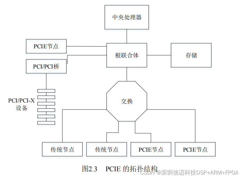
Topology
A typical PCIe fabric consists of a Root Complex (RC), optional Switches, and one or more Endpoints (EP). The RC is the host bridge — it assigns bus numbers, device numbers, and function numbers to all PCIe nodes, and manages interrupt control and hot-plug. Switches forward PCIe packets between ports based on packet destination ID or priority. For backward compatibility, PCIe systems include a PCI Express–PCI bridge to communicate with legacy PCI devices.
Protocol Layering
PCIe uses a three-layer model:
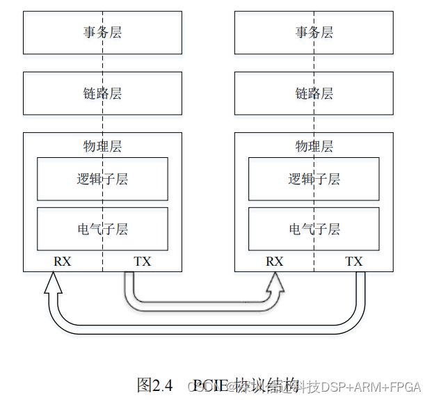
- Transaction Layer — the highest layer, responsible for defining transaction types (Memory Read/Write, I/O, Configuration, Messages). On the transmit side it assembles Transaction Layer Packets (TLPs); on the receive side it unpacks TLPs and passes data to the device core.
- Data Link Layer — ensures packet integrity. Transmit side wraps TLPs into DLLPs by adding sequence numbers and LCRC for error detection; receive side checks these fields and requests retransmission on error.
- Physical Layer — split into a logical sublayer (encoding, link training, lane management) and an electrical sublayer (differential analog interface). PCIe 1.0/2.0 uses 8b/10b encoding at the physical layer.
Packet Format
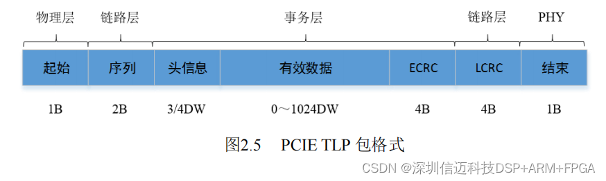
A TLP carries: start byte (physical layer), sequence number (link layer), 3DW or 4DW header (transaction layer), optional ECRC, payload up to 1024 DW (4096 bytes), LCRC (link layer), and end byte (physical layer). Payloads are optional — control transactions carry no data payload.
Configuration Space
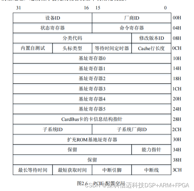
The configuration space is the mechanism for PCIe plug-and-play. Compared to PCI's 256-byte configuration space, PCIe extends this to 4 KB. The header region contains Vendor ID, Device ID, Class Code, and Cache Line Size — fields the OS reads to detect and classify the device. Base Address Registers (BARs) expose the device's memory-mapped I/O regions to the host. The Expansion ROM Base Address Register holds the start address of the device's initialization firmware. This 4 KB space also accommodates PCIe-specific extended capability structures (e.g., Advanced Error Reporting, Power Management).
2.3.2 Aurora Protocol
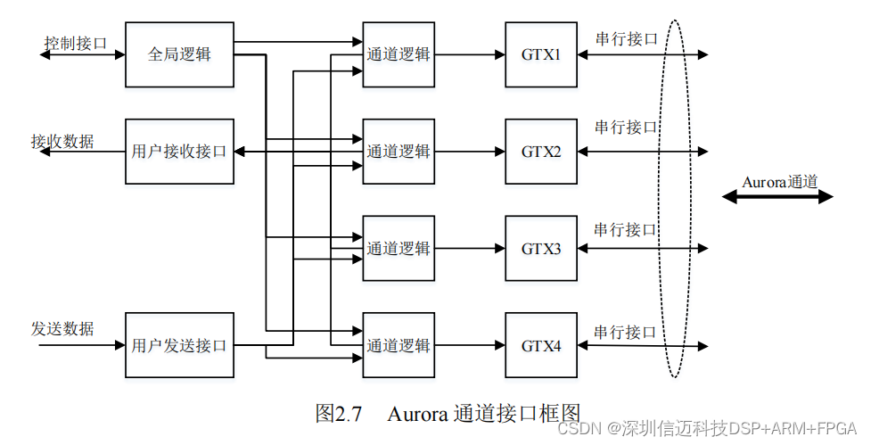
Aurora is a lightweight, point-to-point, scalable serial link protocol originally introduced by Xilinx in 2002, designed specifically for high-speed FPGA-to-FPGA communication. On Xilinx 7-series and UltraScale devices it leverages the GTX/GTH high-speed serial transceivers built into the silicon.
Key characteristics:
- Flexible lane width: a single Aurora link can use 1 to 16 lanes; lanes can be bonded (e.g., x2, x4) to multiply bandwidth. This design uses 4 lanes at 10 Gbps each for a total of 40 Gbps fiber throughput.
- Two simplex modes and full-duplex mode: for unidirectional bulk data streaming (the dominant use case here), simplex TX mode eliminates overhead associated with bidirectional operation.
- Protocol transparency: Aurora is transparent to upper-layer protocols. TCP/IP, UDP, and custom binary streams pass through unchanged — Aurora provides the transport, not the semantics.
- AXI-Stream interface: the user-facing interface follows AXI4-Stream, making it straightforward to connect Aurora to other AXI-native Xilinx IP cores (DMA engines, FIFOs, etc.).
- Encoding: Xilinx's Aurora IP core offers 8b/10b or 64b/66b encoding. This design selects 64b/66b, which has only ~3% encoding overhead versus ~20% for 8b/10b, delivering meaningfully higher effective bandwidth at the same line rate.
Aurora supports two transfer modes:
- Framed mode — data is encapsulated in frames with explicit start-of-frame (SOF) and end-of-frame (EOF) markers. The frame header occupies 2 bytes (K28.2/K27.7 =
0x5CFB) and the frame tail occupies 2 bytes (K29.7/K30.7 =0xFDFE). If a payload has an odd byte count, Aurora pads it to the next even boundary using0x9C. - Streaming mode — continuous data with no framing overhead. No special characters are inserted, reducing resource usage and latency. For high-throughput bulk acquisition like this radar application, streaming mode is the natural choice.
Summary
Part 1 of this series has established the full architectural context for the Zynq-based radar acquisition card: a 1.6 Gsps / 12-bit ADC daughter card feeds data at up to 19.2 Gbps through an FMC connector into the Zynq PL, where asynchronous FIFOs bridge between the ADC, DDR3 buffer, Aurora fiber receiver, and PCIe endpoint modules. The PCIe 2.0 x8 host interface and 4-channel 10 Gbps Aurora fiber link both operate at 40 Gbps raw bandwidth, providing substantial margin over the minimum throughput requirement. Subsequent parts of this series will dive into the detailed RTL implementation of each logic module, the Linux kernel bring-up on the Zynq PS, and the WinDriver-based host PC application.