[Domestic Virtual Instrument] Design of a Dual-Channel 6.4GSPS High-Speed Data Acquisition Module Based on FPGA and JESD204B Clocking (Part 1) Overall Scheme
Designing high-speed data acquisition (DAQ) modules is a complex endeavor, especially when targeting demanding applications like virtual instruments that require exceptional sampling rates and precision. This post, the first in a series, delves into the overall design scheme for a dual-channel 6.4 GSPS high-speed data acquisition module. We will explore the critical specifications, analyze different Analog-to-Digital Converter (ADC) selection strategies, detail the analog front-end design, discuss the intricate JESD204B clocking requirements, and outline the high-capacity data storage solution necessary to handle the immense data throughput.
2.1 High-Speed Data Acquisition Module Specifications and Scheme Analysis
The foundation of any high-performance DAQ system lies in its core specifications. For this module, designed to operate within an AXIe test bus platform, the following key technical parameters define its capabilities and guide the subsequent design choices.
2.1.1 High-Speed Data Acquisition Specifications
The main technical specifications for the high-speed data acquisition module based on the AXIe test bus platform are as follows:
- Maximum Sampling Rate: 6.4 GSPS
- ADC Resolution: 12 bits
- Number of Channels: 2
- Analog Input Bandwidth: 1 GHz
- Coupling: DC
- Input Signal Amplitude: 125 mV, 250 mV, 500 mV, 1 V
- Signal-to-Noise Ratio (SNR): 54 dB @ 380 MHz
- Storage Depth: 2 Gpts
- Transmission: Supports PCIe 2.0 version, four-lane, 5.0 Gbps interface protocol as per AXIe
2.1.2 High-Speed Data Acquisition Scheme
The initial step in any data acquisition process is the digitization of analog signals. Only after this conversion can the digital data be buffered, filtered, and transmitted for further processing. The ADC is the most critical component in a DAQ module, as its performance directly dictates the overall system's capabilities.
For applications requiring very high sampling rates, especially when a single ADC cannot meet the target, techniques like equivalent sampling or time-interleaved sampling are often employed. Equivalent sampling is primarily suitable for repetitive periodic signals, which limits its general applicability. Time-interleaved sampling, however, has no such signal restrictions and is therefore more widely used.
Time-Interleaved Sampling: This technique involves multiple ADCs simultaneously sampling the same analog signal. Each ADC is driven by a sampling clock with a fixed phase difference relative to the others. The data sampled by each ADC is then reassembled in chronological order by a backend receiver, effectively increasing the system's overall sampling rate to the sum of the individual ADC sampling rates.
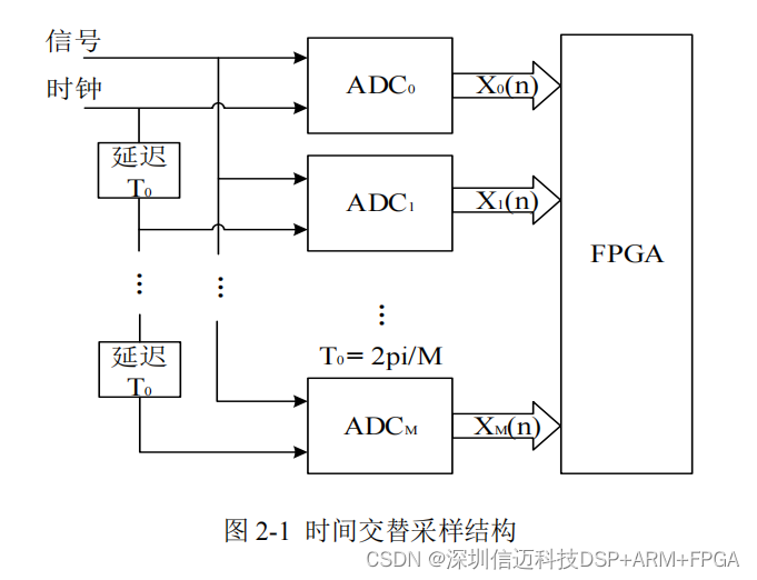
Figure 2-1: Time-Interleaved Sampling Structure
Based on the specified sampling rate (6.4 GSPS) and resolution (12 bits), two suitable ADC chips were identified from the official websites of TI and ADI: the ADC12D1600 and the ADC12DJ3200.
- ADC12D1600: This chip has a maximum sampling rate of 3.2 GSPS and 12-bit resolution. It can achieve 6.4 GSPS through time-interleaved sampling.
- ADC12DJ3200: This chip natively supports a maximum sampling rate of 6.4 GSPS and 12-bit resolution.
Both ADCs can meet the module's sampling rate and resolution requirements. Let's discuss the implementation schemes for achieving 6.4 GSPS with each.
Scheme 1: Using ADC12D1600 The ADC12D1600 integrates two ADC cores and supports two operating modes: single-edge sampling and dual-edge sampling.
- In single-edge sampling mode, the two ADC cores sample their respective input channels on the rising edge of the clock, achieving a maximum sampling rate of 1.6 GSPS per channel.
- In dual-edge sampling mode, the two ADC cores sample the same input channel on both the rising and falling edges of the clock, achieving a maximum sampling rate of 3.2 GSPS.
The ADC12D1600 uses an LVDS parallel interface for data output. Each 12-bit data sample requires 12 pairs of LVDS differential lines. Additionally, a synchronous clock signal (a pair of clock differential lines) is needed for the FPGA to receive and process the sampled data.
To achieve 6.4 GSPS sampling with the ADC12D1600, two such chips are used in a time-interleaved configuration, as shown in Figure 2-2. The analog signal is split into two paths and fed into the inputs of the two ADCs. Both ADCs operate in dual-edge sampling mode, with their sampling clocks at 1.6 GHz and a 90° phase difference between them. The sampled data is then transmitted via LVDS parallel interfaces to the backend, where it is reassembled in chronological order to complete 6.4 GSPS, 12-bit data acquisition.
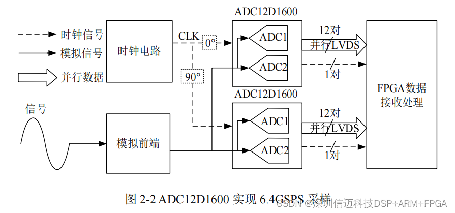
Figure 2-2: 6.4 GSPS Sampling Scheme with ADC12D1600
Scheme 2: Using ADC12DJ3200 The ADC12DJ3200 chip integrates three ADC cores: ADC A, ADC B, and ADC C. ADC C is typically used for backend error correction, periodically replacing ADC A or ADC B to ensure continuous acquisition. Similar to the ADC12D1600, the ADC12DJ3200 also has two operating modes. When operating in dual-edge sampling (single-channel) mode, it can achieve a maximum sampling rate of 6.4 GSPS.
To handle the increased data rates, the ADC12DJ3200 utilizes the JESD204B data output interface. JESD204B employs Clock Data Recovery (CDR) technology, which recovers the clock from the data stream itself, thus eliminating the need for a separate clock line. The ADC12DJ3200 supports up to 16 data transmission lanes. In single-channel mode, it can be configured for 8 or 16 lanes.
Since there is no explicit synchronous clock signal, JESD204B Subclass 1 achieves synchronization through a system reference clock (SYSREF) and a synchronization signal (SYNC). Therefore, for a DAQ module using JESD204B Subclass 1, the clocking circuit must provide not only the device clocks for the ADC and FPGA (for data sampling, deserialization, and recovery) but also a system reference clock to generate derived clocks, which, along with the SYNC signal, establish and maintain the JESD204B link. Figure 2-3 illustrates the 6.4 GSPS sampling scheme using the ADC12DJ3200.
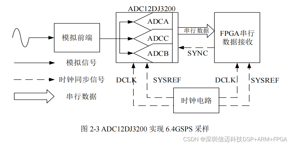
Figure 2-3: 6.4 GSPS Sampling Scheme with ADC12DJ3200
Analog Front-End Design
The analog front-end (AFE) is crucial for conditioning the input signal before it reaches the ADC. This includes converting single-ended signals to differential, providing programmable gain, and ensuring impedance matching.
The LMH5401 is a fully differential amplifier that allows gain to be set using external resistors. It can achieve a maximum signal bandwidth of 6 GHz at a gain of 4 V/V (12 dB). In this design, the LMH5401 is used to convert the DC-coupled single-ended input signal into a differential signal. As shown in Figure 2-4, the ground connection is made through a resistor of the same value as the input source resistance, ensuring that the input impedance matches the given source impedance.
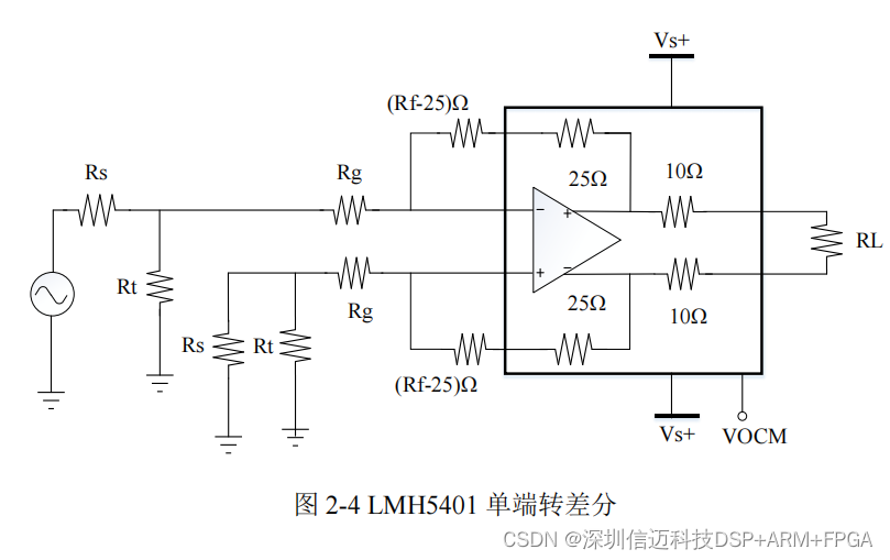
Figure 2-4: LMH5401 Single-Ended to Differential Conversion Circuit
Following the LMH5401, a programmable gain amplifier (PGA) is often used to adjust the signal amplitude to optimize the ADC's input range. The interface between the LMH5401 output and the LMH6401 input introduces a voltage loss of 1.61 dB. Therefore, the voltage gain range before the internal 10 Ω resistor of the LMH6401 is -1.61 dB to 30.39 dB. Considering an additional 6 dB loss at the input, the effective input voltage gain range becomes -7.61 dB to 24.39 dB, which satisfies the required 0 dB to 18 dB gain range for the module.
The specific gain settings for the LMH6401 corresponding to different input voltage ranges are summarized in Table 2-1.
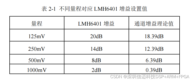
Table 2-1: LMH6401 Gain Settings for Different Input Ranges
2.3 High-Speed Sampling Clock Scheme
The performance of an ADC chip is profoundly affected by the quality of its clock signal. Therefore, ensuring a high-quality clock signal is paramount for the overall data acquisition module. The ADC selection discussion highlighted a major difference between the two data interface types: clocking.
- LVDS Parallel Transmission: In systems using LVDS parallel transmission, the high-frequency sampling clock is fed into the ADC's internal circuitry to drive data acquisition. The ADC then generates a synchronous clock signal, which is sent along with the sampled data to the FPGA. This synchronous clock serves as the primary clock for data reception and processing within the FPGA.
- JESD204B Serial Transmission: Unlike LVDS, JESD204B serial transmission systems require separate device clocks: one for the ADC (DCLK A) and one for the FPGA (DCLK B). While these two clocks can have different frequencies, they must be derived from a common source to maintain synchronization. Beyond these device clocks, the JESD204B standard also mandates other signals for synchronization.
JESD204B Subclass 1 specifically requires a System Reference (SYSREF) signal at both the ADC and FPGA ends, as well as a SYNC signal to establish and maintain the link synchronization between the ADC and FPGA. Typically, JESD204B Subclass 1 only requires device clocks and SYSREF. However, depending on the FPGA model and the speed of the JESD204B link, a global clock might also be necessary at the FPGA end.
The ADC12DJ3200, chosen for its native 6.4 GSPS capability, employs a JESD204B Subclass 1 data transmission interface. Figure 2-6 illustrates a typical JESD204B Subclass 1 clock system, which includes the Device Clock (DCLK), System Reference (SYSREF), Frame Clock (FC), Local Multi-Frame Clock (LMFC), and Global Clock (glbclk).
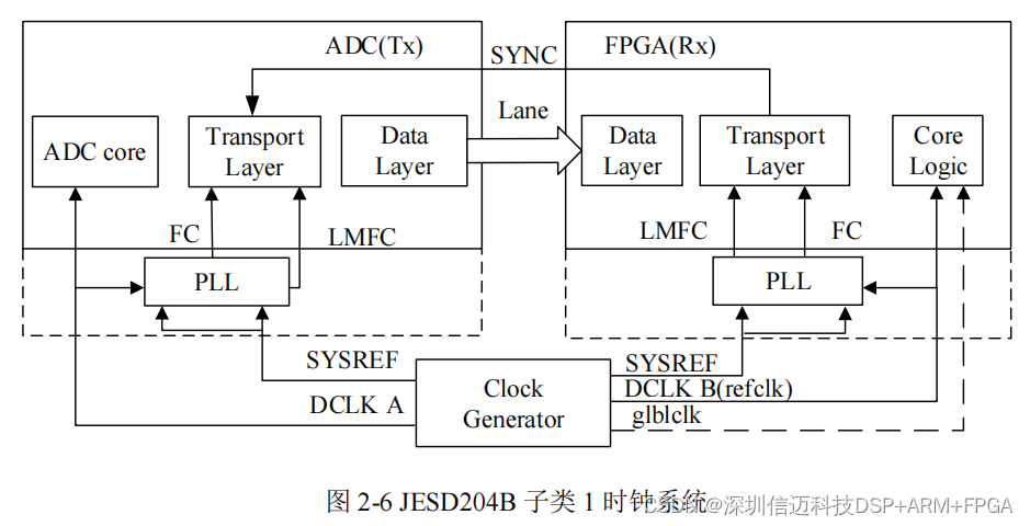
Figure 2-6: Typical JESD204B Subclass 1 Clock System
The Device Clock fed into the ADC (DCLK A) is also known as the sampling clock, used for ADC sampling. The Device Clock fed into the FPGA (DCLK B) is referred to as the reference clock (refclk). This reference clock is essential for the proper operation of the JESD204B physical layer, specifically the GTP/GTX/GTH serial high-speed transceivers within the FPGA. The frequency of this reference clock is determined by the Serial Line Rate, with multiple selectable values available for a given line rate.
The Serial Line Rate refers to the data transmission rate of each lane in the JESD204B link. The general formula for calculating this value is given by Equation (2-5):
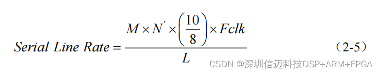
Equation 2-5: General Serial Line Rate Calculation
Where:
- M represents the number of converters on the link.
- N' represents the number of information bits per sample, including sample resolution, control bits, and termination bits.
- Fclk represents the device or sampling clock frequency.
- L represents the number of lanes.
- 10/8 represents the 8b/10b encoding link overhead.
For the ADC12DJ3200 device used in this design, the serial line rate can also be determined using Equation (2-6), as the ADC12DJ3200 defines 18 JESD204B link operating modes, known as JMODEs, with associated parameters.

Equation 2-6: ADC12DJ3200 Specific Serial Line Rate Calculation
In Equation (2-6), DCLK Frequency is the ADC sampling clock, and R is the number of bits transmitted per channel per sampling period. For our system with a 6.4 GSPS sampling rate, when the ADC operates in JMODE1, the sampling clock (DCLK Frequency) is half the sampling rate, i.e., 3.2 GHz, and R is 2. Therefore, the serial line rate is 6.4 Gbps.
2.3.2 Clock Parameter Calculation
From the JESD204B clock system diagram, it's evident that the Frame Clock, Multi-Frame Clock, and other clocks are derived from the device clock. These clocks have specific numerical relationships with the device clock, as depicted in Figure 2-7.

Figure 2-7: JESD204B Clock Relationships
As shown in Figure 2-7, the serial line rate is a crucial parameter in the JESD204B clock system, as the frequencies of all other clocks are related to it. Let's detail the purpose and calculation methods for these clocks, starting with those present at both the ADC and FPGA ends, followed by FPGA-specific clocks.
Byte Clock: The Byte Clock represents the byte rate of the data transmission lane. For DC balancing, the JESD204B data link layer employs 8b/10b encoding. The serial data on the transmission lane consists of 10-bit encoded data for every 8 bits of transmitted data. Thus, the byte clock frequency can be calculated from the serial line rate using Equation (2-7):
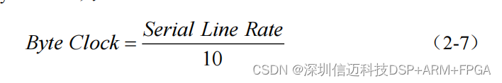
Equation 2-7: Byte Clock Calculation
For this design, the Byte Clock frequency is 640 MHz (6.4 Gbps / 10 bits/byte = 640 MBps, or 640 MHz clock).
Frame Clock: The Frame Clock is the transmission rate of JESD204B data frames. JESD204B packages transmitted data into frames, with each frame containing a specified number of bytes. The Frame Clock frequency can be calculated from either the Byte Clock or the Serial Line Rate using Equation (2-8), where F represents the number of bytes per frame:

Equation 2-8: Frame Clock Calculation
In this design, if F is 8 bytes per frame, then the Frame Clock frequency is 80 MHz (640 MHz / 8 bytes/frame = 80 MHz). The Frame Clock is a divided version of the device clock.
2.4 Data Storage Structure Scheme
The high-speed data acquisition module features two channels, each with a sampling rate of 6.4 GSPS and a resolution of 12 bits. To simplify data handling and align with common memory architectures, the data bit width is expanded to 16 bits per sample. This results in a substantial waveform data rate:
6.4 GSPS × 16 bits/sample × 2 channels = 204.8 Gbits/s = 25.6 GB/s
To accommodate this immense data throughput, a high-speed, large-capacity storage solution is essential. FPGAs typically interface with DDR (Double Data Rate) SDRAM for external memory. A single DDR memory controller interface in an FPGA usually supports a maximum data width of 64 bits. If we were to use a 64-bit wide DDR to achieve the required 25.6 GB/s throughput, the DDR data rate would need to be:
25.6 GB/s / (64 bits / 8 bits/byte) = 25.6 GB/s / 8 bytes = 3.2 GB/s = 3200 MT/s
While DDR4 SDRAM can achieve data rates up to 3200 MT/s, this represents its theoretical maximum. DDR memory requires periodic "refresh" cycles, which temporarily halt normal memory access and reduce operational efficiency. Therefore, a significant margin must be accounted for when calculating DDR data rates. Relying on a 3200 MT/s DDR4 without margin would not meet the continuous throughput demands.
When the required data rate exceeds the maximum sustainable rate of a single DDR interface, the solution is to widen the DDR memory's data bus. By extending the data bus width from 64 bits to 128 bits, the effective DDR data rate required drops significantly:
25.6 GB/s / (128 bits / 8 bits/byte) = 25.6 GB/s / 16 bytes = 1.6 GB/s = 1600 MT/s
This 128-bit wide storage can be implemented using two 64-bit wide DDR devices, with each channel's data corresponding to one DDR. Calculating the data rate for a single DDR (for one channel):
(6.4 GSPS × 16 bits/sample) / (64 bits / 8 bits/byte) = 12.8 GB/s / 8 bytes = 1.6 GB/s = 1600 MT/s
A data rate of 1600 MT/s is well within the capabilities of DDR3 SDRAM, which typically supports up to 2133 MT/s. Again, considering the DDR's refresh time and assuming an access efficiency of 91.03%, the effective DDR3 data rate should be at least 1757 MT/s. Ultimately, DDR3 memory with a data rate of 1866 MT/s was selected as the external storage device.
There were two primary implementation options for using DDR3:
- DDR3 Chips: Employ eight 16-bit wide DDR3 chips, each rated at 1866 MT/s. These would be arranged with four chips in parallel for each channel's data storage. With individual DDR3 chips offering up to 4000 Mb capacity, four chips in parallel per channel could provide 2 GB of storage, meeting the capacity requirement.
- DDR3 Memory Modules (DIMMs): Utilize two 64-bit wide DDR3 memory modules, each rated at 1866 MT/s, with one module dedicated to each channel. DDR3 memory modules can offer capacities up to 8 GB, easily satisfying the storage depth requirement.
Both solutions meet the data rate and capacity requirements. The main difference lies in the circuit design: DDR chips are directly soldered onto the PCB, while DDR memory modules use sockets, which offer greater flexibility for component replacement. Given the advantages of modularity and ease of maintenance, the latter approach was chosen.
The final selection is the Micron DDR3 memory module, model MT8KTF51264HZ-1G9, which offers 4 GBytes of memory capacity, a data rate of 1866 MT/s, and a data width of 64 bits.
The overall storage scheme is illustrated in Figure 2-8. Data acquired from the two ADCs is transmitted via the JESD204B link to the FPGA. Inside the FPGA, the data passes through asynchronous FIFOs for clock domain crossing and initial buffering before entering the storage control module. This module, based on external operation commands and starting addresses, enables continuous multi-segment storage and retrieval. The storage control module will also receive external trigger signals and bidirectional star STRIG trigger signals, along with TRIG[0:11] trigger signals, provided by the AXIe chassis.
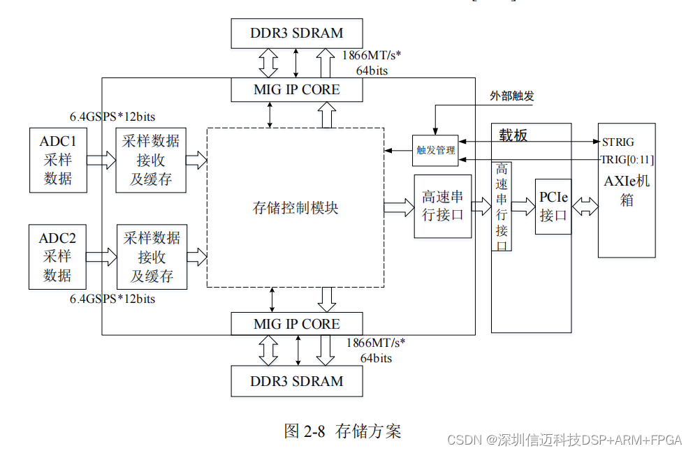
Figure 2-8: Data Storage Architecture