ZYNQ-Based High-Speed IO Control and Nanosecond Synchronous Trigger Signal Generator for Semiconductor Equipment | Precision Process Timing Solution
ZYNQ-Based High-Speed IO Control and Nanosecond Synchronous Trigger Signal Generator for Semiconductor Equipment | Precision Process Timing Solution
📌 Article Summary: Semiconductor lithography, probing, bonding, dicing, and test & sort equipment demand extreme requirements for timing accuracy, multi-channel synchronization, high-speed IO toggling, and precise trigger delays. Traditional MCUs, standard industrial IO cards, and discrete pulse generators suffer from large jitter, poor synchronization, inaccurate delays, and the inability to achieve multi-channel linked triggering. This article leverages the ZYNQ heterogeneous architecture, utilizing the nanosecond-level timing advantages of FPGA (PL) hardware to achieve high-speed parallel IO control, programmable precision delay, and multi-channel synchronous triggering. The ARM (PS) handles process parameter configuration, timing table management, and host PC interaction, perfectly meeting the timing control requirements of semiconductor precision equipment. This is a practical solution for industrial precision timing, high-speed pulse generation, and synchronous triggering systems.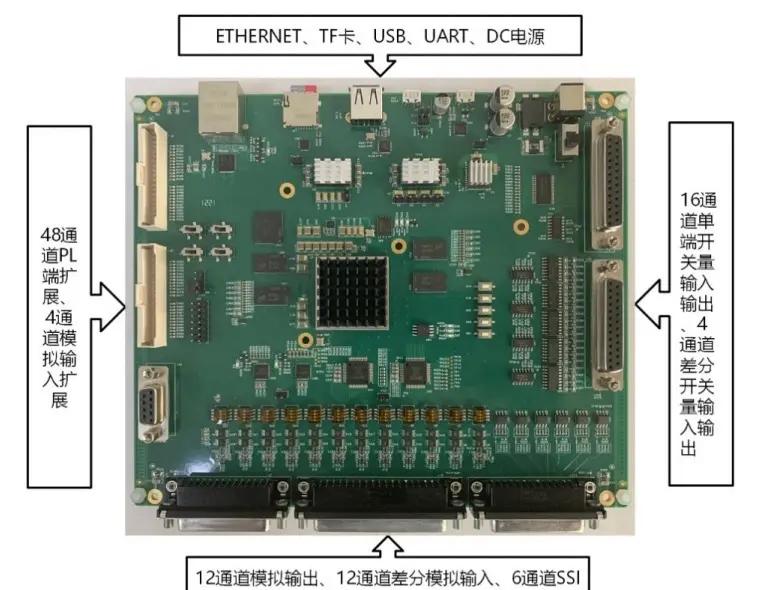
🔑 Keywords: ZYNQ, Semiconductor Equipment, High-Speed IO, Synchronous Trigger, Nanosecond Timing, Pulse Generator, Precision Timing Control
I. Project Background and Industry Pain Points
Semiconductor equipment belongs to the category of ultra-high precision timing-dependent equipment. Whether it's optical exposure, probe testing, wafer handling, laser marking, or chip sorting, core operations rely on strict timing linkages: light source triggering, camera exposure, motion axis positioning, sampling initiation, and laser emission must achieve zero timing deviation, extremely low jitter, and precisely controllable delays.
Current industry control solutions have obvious shortcomings and cannot meet semiconductor process requirements:
-
MCU/ARM Bare-Metal IO Control: Software-toggled IO exhibits microsecond-level jitter, and scheduling delays are uncertain, making nanosecond-level precise triggering impossible.
-
Commercial Pulse Generators/Timing Cards: Expensive, fixed functionality, difficult for secondary development, and hard to adapt to customized equipment timing logic.
-
Discrete Timing Chip Solutions: Many peripheral components, complex wiring, poor channel scalability, and difficulty in multi-device synchronization.
-
Pure FPGA Solutions: Cumbersome parameter configuration, timing table management, and device networking interaction, with weak human-machine interaction and remote operation & maintenance capabilities.
The ZYNQ heterogeneous architecture perfectly suits semiconductor precision timing scenarios: The PL-side hardware logic has no operating system jitter, enabling nanosecond-level high-speed IO and precise triggering; the PS-side Linux system flexibly manages timing parameters, trigger sequences, and communication protocols, balancing ultimate real-time performance with software flexibility. It is a lightweight and cost-effective solution for semiconductor equipment timing control.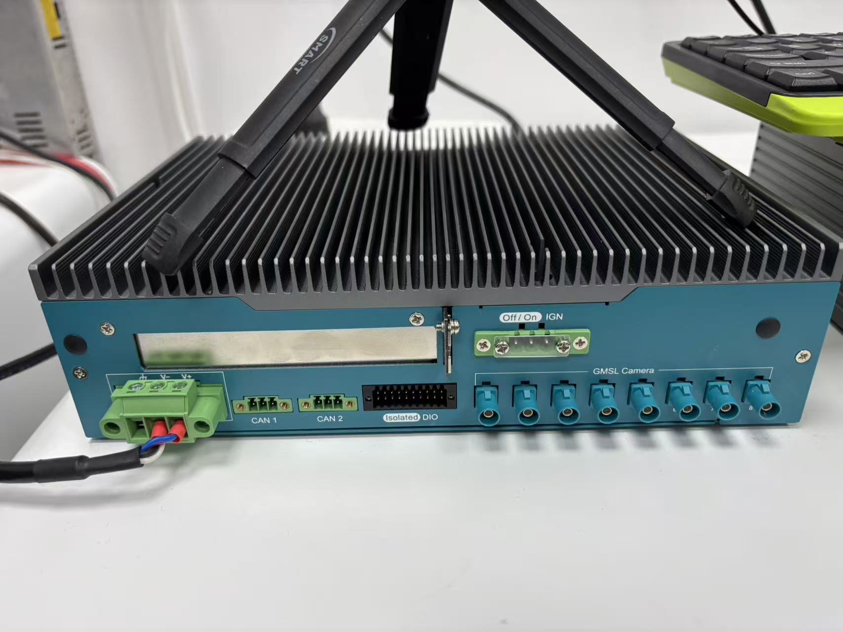
II. System Core Design Metrics
This high-speed IO and synchronous trigger system is benchmarked against entry-level precision timing controllers for semiconductor equipment, with core metrics as follows:
-
Timing Accuracy: Hardware nanosecond-level timing resolution, trigger jitter < 5ns, meeting the requirements for optical and probing precision processes.
-
Channel Capability: Supports multiple independent high-speed IO channels, configurable for input sampling, pulse output, and synchronous triggering.
-
Delay Configuration: Supports independent programmable delay for any channel, precisely controlling trigger timing differences.
-
Trigger Modes: Supports software immediate trigger, external hardware trigger, multi-channel linked chain trigger, and periodic automatic trigger.
-
IO Speed: High-speed IO toggling frequency up to hundreds of MHz, supporting precise narrow pulse output.
-
Synchronization Capability: Global clock synchronization, extremely low multi-channel trigger timing deviation, no phase shift.
-
Scalability: Supports programmable timing sequence configuration, switching between multiple trigger schemes, Ethernet parameter download, and status monitoring.
III. Overall System Architecture Design
The system adopts the classic ZYNQ PS+PL heterogeneous hardware-software co-design architecture, strictly separating the real-time timing layer from the business management layer, perfectly matching the "hard real-time timing + flexible parameter configuration" requirements of semiconductor equipment.
3.1 FPGA (PL) Core Real-time Layer
-
PLL/MMCM frequency multiplication generates a high-precision, low-jitter global clock, establishing a nanosecond-level timing reference.
-
Multi-channel high-speed IO parallel driving enables high-speed pulse output and external trigger signal acquisition.
-
Hardware delay chains and timing counters achieve programmable precise delay triggering.
-
Multi-channel synchronous trigger logic and chain trigger state machines complete complex timing linkages.
-
Trigger status, IO status, and count values are real-time mapped to the PS side via AXI registers.
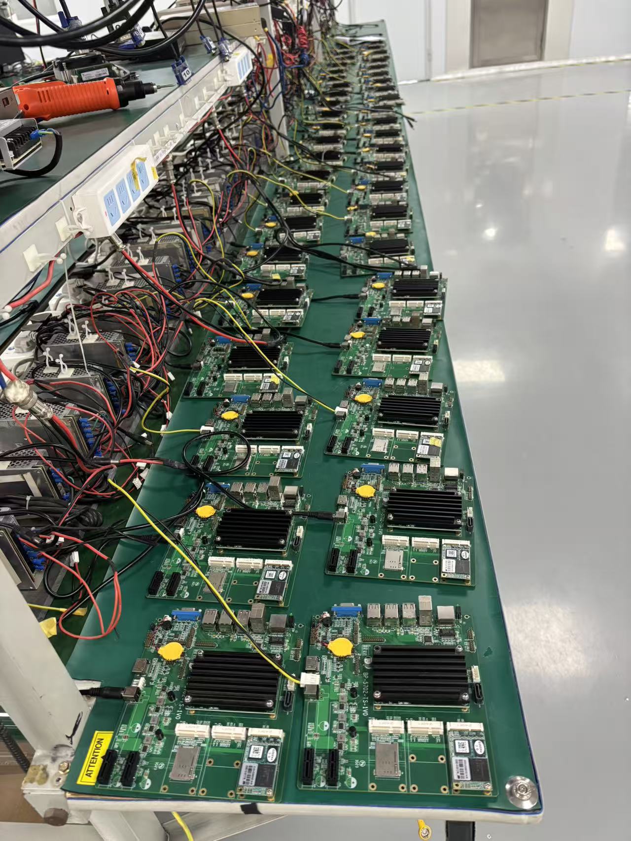
3.2 ARM (PS) Core Business Layer
-
Configuration download of timing parameters, delay parameters, pulse width, and trigger period.
-
Storage, switching, and calling of multiple process timing schemes.
-
Reading PL-side IO status, trigger count, and timing anomaly status.
-
Ethernet/serial port receives host PC commands, reports device timing operation status.
-
Exception protection: automatic interlocking and alarming for timing errors and signal anomalies.
3.3 Overall Data Flow and Timing Flow
Host PC timing parameters download → ARM configures timing table and trigger parameters → AXI bus writes to PL registers → FPGA hardware timing logic generates precise trigger pulses/IO levels → Drives semiconductor equipment optical/motion/sampling units → External feedback signal re-sampling and verification → Status feedback to ARM for reporting to host PC.
IV. FPGA Core Precision Timing Design (Core Technology)
4.1 Low-Jitter Global Clock Architecture
Semiconductor timing control is extremely sensitive to clock jitter. This design abandons the scheme of directly driving logic with an external crystal oscillator, instead using PL internal MMCM/PLL clock frequency multiplication and shaping to generate a highly stable, low-jitter global clock. This serves as the unified timing reference for all IO triggers, delay counting, and pulse generation, ensuring timing accuracy at the source.
4.2 Nanosecond Programmable Delay Trigger Mechanism
The system builds hardware timing counters and delay comparison logic on the FPGA side. The PS side can configure the absolute trigger delay, pulse width, and trigger interval for any channel. The PL side real-time compares the current clock count value with the preset trigger value, immediately toggling the IO upon reaching the set time. This is full hardware execution, without software intervention or scheduling jitter, achieving precise nanosecond-level delay control, perfectly suited for laser triggering, camera exposure, and AD synchronous sampling scenarios.
4.3 Multi-Mode Trigger Logic Implementation
To address the multi-scenario process requirements of semiconductor equipment, four common industrial trigger modes are implemented:
-
Software Single Trigger: Host PC command triggers immediately, used for single-point debugging and equipment calibration.
-
External Hardware Trigger: Receives sensor, home position, or arrival signals, linking to trigger subsequent processes.
-
Periodic Automatic Trigger: Programmable periodic pulse output, used for continuous processes and repetitive operations.
-
Multi-Channel Chain Trigger: After channel A triggers, channels B/C are triggered after a fixed delay, achieving multi-process timing linkage.
4.4 High-Speed IO Electrical and Timing Constraint Optimization
To address high-speed IO signal integrity issues, strict timing constraints are completed in Vivado: global clock constraints, maximum IO delay constraints, and input/output delay constraints. Simultaneously, FPGA IOB registers are used to register signals, reducing routing delay deviations and preventing high-speed signal distortion and trigger offset, ensuring timing consistency for each IO trigger.
V. ARM Software Architecture Design
5.1 Parameter Configuration and Timing Table Management
The ARM side builds multiple sets of timing configuration tables, which can store pulse width, trigger delay, trigger mode, and channel enable parameters for different processes. It supports one-key switching of process schemes, adapting to various process scenarios such as wafer testing, optical inspection, and laser processing.
5.2 AXI High-Speed Parameter Interaction
Interaction with the PL side is achieved via the AXI-GP high-speed register interface, allowing for rapid download of timing parameters and reading of real-time status with extremely low interaction latency. It supports dynamic online modification of timing parameters without needing to restart the device, improving debugging and production efficiency.
5.3 Status Monitoring and Exception Protection
The software real-time monitors trigger status, IO level