FPGA-based Single-Board Miniaturized Digital Interference Source, Capable of Generating Arbitrary IF Frequency Output from 500MHz to 3000MHz
The XM250M3G is a single-board miniaturized digital interference source designed for electronic countermeasure (ECM) applications. Built around an FPGA signal-processing core, it generates arbitrary intermediate-frequency (IF) output anywhere in the 500 MHz–3000 MHz band and supports selectable instantaneous bandwidths up to 250 MHz — all within a compact module the size of a credit card. This post covers the board's architecture, key specifications, and the practical engineering trade-offs that make it useful in airborne, vehicle-mounted, and ground-based jamming systems.
What Is a Digital Interference Source?
Traditional analog jammers generate noise or tone signals using VCO/PLL chains and analog noise sources. A digital interference source replaces that analog back-end with an FPGA (or DSP+FPGA combination) that synthesizes the interference waveform in the digital domain, then converts it to the analog IF through a high-speed DAC. This approach offers several concrete advantages:
- Waveform agility: the FPGA can switch between Gaussian white noise, comb spectra, or custom modulation patterns by reprogramming internal coefficients — no hardware swap required.
- Precise bandwidth control: instantaneous bandwidth is set digitally (typically by adjusting a digital filter's passband), so it can be changed on the fly over a control link.
- Repeatable power calibration: output power is determined by DAC full-scale and programmable gain stages, making it far easier to hit a consistent dBm target across temperature.
The XM250M3G packages all of this into a 68 mm × 42 mm × 8 mm single-board module — small enough to integrate into existing rack systems, UAV payloads, or handheld ECM kits.
Technical Specifications
| Parameter | Value |
|---|---|
| Output frequency range | 500 MHz – 3000 MHz |
| Instantaneous interference bandwidth | 50 / 100 / 150 / 200 / 250 MHz (selectable) |
| Interference waveform types | Gaussian white noise, comb spectrum |
| Output power | ≥ −15 dBm |
| Input signal range | −25 dBm to 0 dBm |
| Power supply | +12 V / 0.5 A |
| Control interface | RS-422 |
| Board dimensions | 68 mm × 42 mm × 8 mm |
Output Frequency Range: 500 MHz – 3000 MHz
This 2.5 GHz span covers many tactically relevant frequency bands: UHF communications (around 400–500 MHz edge), L-band radar and GPS (1–2 GHz), S-band radar (2–4 GHz), and common datalink and telemetry frequencies. The board produces an IF output — it does not up-convert to the final RF frequency itself. The downstream RF chain (mixer, local oscillator, bandpass filter, and power amplifier) performs the final frequency translation to the target emission band. This two-stage architecture is standard practice: keeping the digital board at IF frequencies reduces the DAC sample-rate requirements, simplifies board layout, and isolates sensitive digital logic from high-power RF.
Instantaneous Bandwidth: 50 MHz to 250 MHz
Selectable in five steps (50/100/150/200/250 MHz), the instantaneous bandwidth parameter determines how wide a frequency slice is jammed at any given moment. Wider bandwidth covers more of the target's spread-spectrum or frequency-hopping range simultaneously but dilutes power spectral density — meaning less jamming power per hertz. Narrower bandwidth concentrates power but may miss fast-hopping targets. The ability to switch this parameter via the RS-422 control interface lets the system operator (or an onboard controller) adapt to the threat environment in real time.
Interference Waveform: Gaussian White Noise and Comb Spectrum
Gaussian white noise (also called barrage noise jamming) spreads energy uniformly across the selected bandwidth. It degrades receiver SNR in a predictable way and is effective against narrowband communications, radar receivers, and analog systems where the noise floor matters most. In an FPGA implementation, Gaussian noise is typically generated using a pseudo-random bit sequence (PRBS) filtered by a digital noise-shaping filter to approximate the Gaussian amplitude distribution, then band-limited to the selected instantaneous bandwidth.
Comb spectrum jamming places discrete tones at regular frequency spacings across the band — resembling a comb when viewed on a spectrum analyzer. This mode is particularly effective against certain narrowband hopping radios and OFDM systems, where individual tones can capture specific subcarriers or synchronization channels. Switching between the two modes on the XM250M3G is handled at the FPGA firmware level without any analog hardware change.
Power Budget: +12 V at 0.5 A
The 6 W power envelope is tight for a board spanning 500 MHz–3000 MHz, and reflects the efficiency of modern FPGA fabric combined with high-speed DAC technology. The output power of ≥ −15 dBm is the IF output level; the downstream PA chain will add gain (typically 30–60 dB depending on application) to reach the final radiated power. The input signal range of −25 dBm to 0 dBm refers to any reference or trigger input accepted by the board — for example, a pilot tone or synchronization signal fed from the system controller.
Control Interface: RS-422
RS-422 is a differential, half- or full-duplex serial standard capable of multi-drop bus topologies and cable runs up to several hundred meters. It is a common choice in military and embedded defense electronics because it is highly noise-immune (differential signaling rejects common-mode interference), does not require a shared ground, and is supported by virtually every FPGA without external transceivers beyond a simple line driver IC. Commands sent over this bus configure the output frequency, instantaneous bandwidth, waveform type, and output enable state.
Board Dimensions and Form Factor
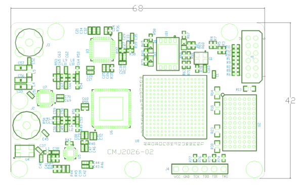
At 68 mm × 42 mm × 8 mm, the XM250M3G fits within a standard half-size mezzanine envelope. The 8 mm height budget (roughly 0.31 inches) suggests the board uses low-profile connectors and thin chip packages — important for stacking in multi-board ECM system assemblies.
Physical Hardware
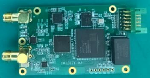
The production board photograph shows a dense layout consistent with a high-speed mixed-signal design: the FPGA likely occupies the largest footprint, flanked by the high-speed DAC, clock generation circuitry, and the RS-422 transceiver. RF connectors (SMA or MCX at this size class) bring the IF output off-board to the downstream up-conversion and amplification chain.
Typical ECM Integration Scenario
In a complete jamming system, the XM250M3G sits at the IF stage of a multi-channel transmit chain:
- System controller sends waveform parameters (frequency, bandwidth, waveform type) over RS-422.
- XM250M3G synthesizes the digital waveform, converts it to analog IF, and outputs it at ≥ −15 dBm.
- Up-converter mixes the IF signal with a programmable local oscillator to reach the target RF frequency band.
- Power amplifier boosts the signal to the required radiated power level.
- Antenna (directional or omnidirectional depending on the jamming geometry) radiates the signal.
The single-board miniaturized approach of the XM250M3G reduces system complexity and weight at the most digitally intensive part of this chain — the waveform generator — which is the component most likely to benefit from FPGA-based reconfigurability as threat libraries evolve.