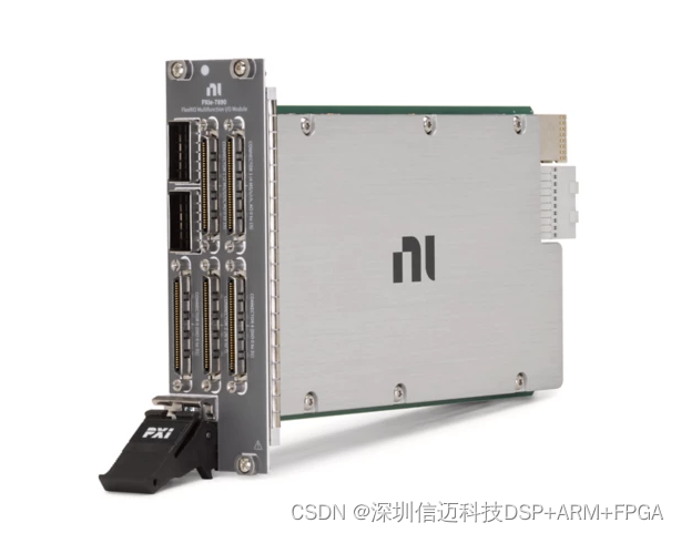
[Domestic Alternative to NI] PXIe-7890 Hardware-in-the-Loop Simulation, 8 AO, 16 Low-Latency AO, 64 DIO, FlexRIO Multifunction I/O Module
A Domestic Alternative for PXI-Based HIL Testing: Inside the PXIe-7890 FlexRIO Multifunction I/O Module
Hardware-in-the-Loop (HIL) simulation sits at the heart of modern power electronics validation — and until recently, NI's FlexRIO family had few credible domestic competitors in the Chinese market. The PXIe-7890 changes that calculus. This article walks through the module's architecture, explains why each I/O resource matters for signal-level inverter HIL, and describes how the card is positioned for ECU verification and validation workflows.
What the PXIe-7890 Is Built For
The PXIe-7890 is a PXI Express multifunction I/O module designed specifically for signal-level inverter Hardware-in-the-Loop (HIL) applications. In a signal-level HIL setup, the real-time simulator must reproduce the fast, low-latency analog signals that an Electronic Control Unit (ECU) would receive from physical sensors and actuators — pulse-width modulation feedback, resolver signals, current sense outputs, and so on — without the actual power stage present. The simulator must be fast enough that the ECU cannot distinguish simulated signals from real ones.
This is a demanding workload. It requires a combination of high-channel-count analog I/O, deterministic digital I/O, and an FPGA fabric that can execute closed-loop control models in microseconds rather than milliseconds. The PXIe-7890 addresses all three requirements in a single PXI Express slot.
I/O Resources at a Glance
The module integrates the following I/O resources:
- 8 channels of Analog Input (AI) — used to digitize sensor feedback from the ECU under test, such as current or voltage measurements returned from the ECU's own output stage
- 8 channels of standard Analog Output (AO) — general-purpose DAC outputs for driving reference signals or emulating sensor voltages presented to the ECU
- 16 channels of low-latency Analog Output (AO) — a dedicated bank of DAC outputs optimized for minimum propagation delay, critical for closing the simulation loop at inverter switching frequencies (typically 4–20 kHz in traction applications)
- 64 channels of Digital I/O (DIO) — high-density digital lines for PWM capture, resolver interface emulation, CAN/SPI bit-bang, or discrete fault injection
- 2 × QSFP high-speed serial ports — quad small form-factor pluggable connectors supporting multi-gigabit serial links for inter-chassis synchronization, real-time data streaming, or connecting to a host simulation PC
The distinction between the 8 standard AO channels and the 16 low-latency AO channels is significant. Standard AO paths typically route through additional filtering and protection circuitry that adds tens of microseconds of group delay. The low-latency bank bypasses much of this conditioning to deliver output updates in the sub-microsecond range — essential when the FPGA is running a motor model and must update the simulated back-EMF voltage within a single PWM switching period.
The FPGA Core: Kintex UltraScale KU060
The computational backbone is a Xilinx (AMD) Kintex UltraScale KU060 FPGA. The KU060 is a mid-to-high-end device in the UltraScale family, offering approximately 725K logic cells, 5,520 DSP slices, and high-speed transceivers capable of multi-gigabit serial I/O — which feeds directly into the two QSFP ports.
For HIL motor simulation, DSP slice count matters more than raw LUT count. A single three-phase traction motor model running at a 1 µs simulation step requires dozens of multiply-accumulate operations per cycle. The KU060's DSP density allows the module to host multiple independent traction motor models simultaneously — for example, simulating a front axle motor, a rear axle motor, and an auxiliary drive in a single FPGA image, synchronized to a common time base.
The FPGA also provides the deterministic I/O scheduling that a CPU-based real-time system cannot match. All analog samples and digital transitions are timestamped and actuated relative to the FPGA's internal clock, eliminating the jitter introduced by OS scheduling or DMA arbitration.
ECU Verification and Validation Workflow
The primary application target is confirming and validating ECU performance — replacing physical motor and inverter hardware with a simulation that the ECU cannot distinguish from the real plant. A typical validation loop looks like this:
- The ECU sends PWM gate drive signals to what it believes is an IGBT inverter bridge.
- The PXIe-7890 DIO channels capture those PWM signals in real time on the FPGA.
- The FPGA executes a motor model (e.g., a d-q axis model of a permanent magnet synchronous motor), computing instantaneous phase currents and back-EMF.
- The computed phase current values are written to the low-latency AO channels as analog voltages, mimicking the output of current sense resistors or Hall-effect sensors.
- The ECU reads those simulated sensor signals on its ADC inputs and closes its own current control loop accordingly.
Because the entire round-trip — PWM capture → model execution → analog output — happens inside the FPGA fabric, latency can be kept to a few microseconds. This is fast enough to run the ECU at full switching frequency without the ECU detecting anomalies in the feedback timing.
The 2 QSFP ports add flexibility for multi-board or multi-chassis configurations where, for example, one PXIe-7890 simulates the powertrain inverter while a second simulates the battery management system, and both must exchange state variables at nanosecond-accurate synchronization.
Positioning as a Domestic NI Alternative
NI's PXIe-7820R, PXIe-7856R, and PXIe-7902 FlexRIO modules have long been the reference standard for this class of application. The PXIe-7890 targets the same socket — PXI Express, FlexRIO-style FPGA-centric I/O, HIL-focused channel mix — while offering a domestically sourced supply chain, which has become a procurement priority for Chinese automotive OEMs and Tier 1 suppliers operating under import substitution pressures.
For engineering teams already familiar with FPGA-based HIL development, the module's KU060 core and mixed I/O complement make it a technically credible drop-in candidate for signal-level inverter HIL rigs, ECU production-line testers, and motor drive R&D benches where full test coverage and repeatable simulation fidelity are non-negotiable requirements.