A Brief Discussion on AM5728 Bare-Metal Debugging
I. A Brief Discussion on ARM Bare-Metal Debugging
-
Connecting the Emulator and Reading/Writing Registers Plug the hardware emulator into the ARM board's JTAG port, then connect it to the PC. Most modern ARM emulators connect to the PC via USB. After connecting, power on the board, then open the debugging software on the PC. Here, I'm using an ARM11 emulator with AXD as the debugging software. If AXD recognizes the ARM processor, the connection is successful; otherwise, there's an issue. (1) Verify that all power supplies to the ARM processor are correct. (2) Verify the ARM processor's RESET pin. (3) Verify that the ARM processor's crystal oscillator is oscillating. (4) Verify the JTAG interface is correct. If all four points above are normal, the emulator should be able to detect the ARM.
-
Initializing the ARM Processor and DRAM via Script Since it's a bare-metal board, the ARM undergoes no initialization after power-on. Typically, a script is executed to perform basic initialization of the ARM. A script is usually a .txt file, for example:
setmem 0x36001004 0x4     32
setmem 0x36001010 0x40d   32
setmem 0x36001014 0x6     32
setmem 0x36001018 0x3     32
setmem 0x3600101c 0xf     32
setmem 0x36001020 0xf     32
setmem 0x36001024 0xf     32
mem 0x36001000 +1         32
mem 0x36001004 +1         32
mem 0x36001008 +1         32
mem 0x3600100c +1         32
….
The script commands above are for AXD software. The "setmem" command sets a value to a specific address, while the "mem" command reads a value from an address and prints it. These two commands allow you to set internal ARM registers and read their values. The main purpose of the script is to initialize the ARM, typically including disabling interrupts and the watchdog, configuring the clock, GPIOs, and the DRAM controller. How do you run a script in AXD? First, in the AXD menu, select "System Views", then "Command Line Interface". A window will pop up; enter the following command:
ob c:/ init .txt
After the script finishes executing, the ARM and DRAM on the board should be initialized. At this point, you can perform memory read/write tests. In the menu, select "Process Views", then "Memory", enter the DRAM address, and modify some values at those addresses. Changed values will turn red. If you can modify them, it indicates that the DRAM is likely working correctly.
- Downloading and Running Programs in DRAM via AXD
Next is downloading the program to DRAM for execution. The main purpose of this program is to flash the bootloader. Modern ARM processors are very powerful and support various boot modes. Depending on the boot mode, the bootloader needs to be flashed to different media. In the AXD menu, select "File", then "Load Memory from File…". A window will pop up, as shown:
As shown, you need to enter the download address in "Address". This address is the execution address for Loader_RAM.bin. After a successful download, open the serial port, then in AXD's "Command Line Interface", enter the command "setpc 0x50000000" to point the Program Counter (PC) to address 0x50000000, and then enter "go" to start execution.
- Flashing the Bootloader and Booting the ARM Board Once the downloaded program is running, it can be used to flash the bootloader to Nandflash, NORflash, or an SD card, depending on the board's supported boot modes. This program can download the bootloader via the serial port. Another method is to pause program execution in AXD, then download the bootloader to DRAM via the emulator, resume program execution in AXD, and use the initially downloaded program to flash the bootloader to flash memory or the SD card. After successful flashing, power off, disconnect the emulator's JTAG, and power on again. At this point, the bootloader in the ARM board should be able to run.
Once the bootloader is running, the task becomes easier. Modern bootloaders are very powerful; Linux has U-Boot, and WinCE has Eboot, both supporting flashing, downloading, and other functions. Typically, if you purchase a development board, a flashing tool will be provided. However, after replacing DRAM and Nandflash, the flashing tool might need re-debugging, and the bootloader used may also require modifications.
Reference: http://www.eeworld.com.cn/mcu/article_2016042525926.html
II. Using a JTAG Debugger
JTAG is used for chip testing and program debugging. JTAG is located inside the CPU. When the CPU sends and receives data on its pins, it passes through the JTAG unit. The JTAG unit exposes four pins from within the CPU: TMS, TCK, TDI, and TDO. These can then be connected to a PC via an OpenJTAG debugger (USB connection) on one end, and to these JTAG pins on the other end to control the CPU.
On a bare-metal S3C2440 board, when booting from NAND, the S3C2440 automatically copies the first 4KB to internal SRAM.
However, at this point, the control timings for SDRAM, NAND flash, etc., have not yet been initialized. Therefore, we can only use addresses 0-4095 (the first 4KB) to initialize SDRAM and NAND flash. Only after initialization is complete can the contents from NAND flash addresses 4096 onwards be loaded into SDRAM.
III. FPGA Power-On Configuration and Initialization
The FPGA's AS (Active Serial) configuration process is mainly divided into three stages: reset, configuration, and initialization. Before configuration, there is a POR (Power-On Reset) process, meaning the FPGA undergoes a POR immediately after power-on before the entire configuration flow begins. The POR duration can be controlled by manipulating the PORSEL pin. When PORSEL is high, the POR duration is approximately 12ms; when PORSEL is low, it's approximately 100ms.
During POR, both nconfig and nstatus are low, entering the reset process. After POR, the FPGA releases the nconfig signal, which is then pulled high by an external pull-up resistor, thereby entering the configuration process.
During the configuration phase, the FPGA generates a DCLK clock. Synchronized with this clock, the FPGA sends configuration commands or addresses to the configuration device and reads configuration data. DCLK can operate at two speeds: 20MHz and 40MHz. The corresponding configuration modes are called AS and Fast AS, respectively. Only configuration devices with a capacity of EPCS16 or higher support Fast AS.
Once all configuration data has been transferred, the FPGA releases the config_done signal. This pin is pulled high by an external 10k resistor. Upon detecting config_done as high, the FPGA enters the initialization process.
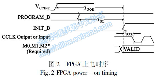
3.1 FPGA Power-On Startup The first step for FPGA operation is to power on the device. Xilinx requires VCCINT (core voltage) to rise first, followed by VCCO (I/O voltage), with the worst-case scenario being a difference of no more than 1 second between them. In parallel configuration mode, VCCO_2 requires the reference voltage to be the same as the PROM reference voltage. The power-on sequence is shown in Figure 2. Here, TPOR (Power-on-Reset) is 5~30ms, T(PL) (Program Latency) is Max 4ms, and T(icck) (CCLK output delay) is Min 500ns.
When the system powers on normally or PROG-B receives a low pulse, the FPGA begins configuring its register space. During this period, all I/O pins, except for the defined configuration pins, are set to a high-impedance (High-Z) state. Multiple tests indicate that this stage takes approximately 30ms.
The final step in the FPGA startup phase is configuring the boot mode. When PROG-B goes high, the FPGA starts sampling the configuration mode pins (M3, M2, M1) and simultaneously drives the CCLK output. During this stage, there are two methods to delay the FPGA's configuration timing: one is to pull the INIT-B pin low, which causes the FPGA to detect that it has not yet completed initialization and will not proceed with subsequent operations until INIT-B goes high. The other is to pull the PROG-B pin low, keeping the FPGA in a waiting-for-configuration state.
3.2 FPGA Data Loading Before normal FPGA data loading, a synchronization check between the device and the PROM is required. This is done by transmitting a special 32-bit value (0xAA995566) to the FPGA, signaling that the subsequent data transfer will be configuration data. This step is transparent to the user because this checksum is automatically included in the .bit file generated by the Xilinx ISE Bitstream Generator.
After completing the pre-configuration communication synchronization, the FPGA and PROM still cannot identify each other's device type. Therefore, Xilinx assigns a unique device ID number to each FPGA model, which can be found in the Xilinx configuration manual. For example, the XC4VS35 used in the example above has an ID of 0x02088093. The FPGA needs to read this device ID from the PROM and compare it with its own. If they match, it proceeds with the next steps; otherwise, configuration fails, and configuration error information is printed.
Once all preparatory work is successfully completed, the FPGA begins loading the configuration file. This step is also transparent to most users and is performed autonomously by the device. This is also the most time-consuming step in the configuration process, ranging from 100ms to several seconds. During this process, all configurable I/Os of the FPGA become weak pull-up (if HSWAPE=1) or high-impedance (if HSWAPE=0) based on the HSWAPEN pin setting. The I/O pins in this stage have not yet transitioned to the user-desired state and are most likely to affect the power-on sequencing and operation of other peripheral circuits. When designing hardware circuits, special attention must be paid, and necessary measures taken, such as adding pull-up/pull-down resistors or changing the device power-on sequence, to minimize or avoid the impact of FPGA configuration on other components in the circuit.
After the configuration