How TI's DSP+ARM Dual-Core Architecture Communicates
1 Introduction to Communication Architecture
To address the complexity of current applications, SoC chips are better equipped to meet application and media demands, integrating numerous interfaces. ARM serves as the application processor for diverse application development, user interfaces, and interactions, while DSP is utilized for algorithm acceleration, particularly for media codec algorithm acceleration. This approach maintains algorithmic flexibility while providing powerful processing capabilities. Following its first series of Davinci chips, the DM644x, Texas Instruments (TI) successively launched a series of ARM+DSP or ARM+video co-processor multimedia processor platforms, including the DM643x, DM35x/36x, DM6467, OMAP35x, and OMAPLx. Many engineers with strong DSP development experience, as well as those with application processing development experience, have transitioned to developing products such as video surveillance, video conferencing, and portable multimedia terminals on Davinci or OMAP platforms. How can one develop and implement desired embedded applications based on an ARM+DSP chip architecture?
Traditional chips typically feature a single processor core, either a general-purpose processor like ARM or a DSP. For control and user interfaces, general-purpose processors are usually employed, while algorithm processing or media processing relies on DSPs or hardware chips. Many systems adopt a dual-chip architecture. The development model is also relatively straightforward; for ARM chips, there are ARM emulation tools, and application development is based on an OS; for DSPs, there are DSP development tools, such as TI's CCS and 510/560 emulators, which allow for algorithm porting, optimization, tracing, and debugging. In these cases, the required expertise is relatively singular.
For ARM+DSP dual-core architectures, many engineers are unsure how to begin development and have raised numerous questions. For ARM engineers, common confusions include how to use DSP resources, how to interact with data, and how to maintain synchronization between the two cores. DSP engineers, on the other hand, ask how to debug ARM, how to start the DSP, and how to operate peripherals to acquire or send data for media acceleration. Based on different development experiences and backgrounds, ARM engineers and DSP engineers view SoC chips from completely different perspectives, often not knowing where to start. Here, I will share my experience.
First, an ARM+DSP chip is dual-core, with ARM and DSP corresponding to different instruction sets and compilers. The SoC chip can be viewed as a combination of two single chips, requiring two sets of different development tools. CCS3.3 can perform chip-level debugging and emulation, but different platforms need to be selected for ARM and DSP. Generally, ARM runs an operating system, such as Linux or WinCE. Development on ARM, apart from the bootloader, is primarily OS-based, including drivers, kernel customization, and upper-layer applications. Debugging and emulation mainly rely on logs or OS-provided debuggers like KGDB and Platform Builder. Development on the DSP core is similar to traditional single-core DSP development, requiring CCS + emulator for development and debugging.
Second, both the ARM and DSP cores can access the chip's peripheral interfaces. Typically, ARM controls all peripherals through OS drivers, similar to traditional ARM chips. The DSP primarily performs algorithm acceleration and mainly interacts with memory. To maintain consistency in chip resource management, it is advisable to avoid DSPs accessing peripherals. Of course, depending on specific application requirements, the DSP can also control peripheral interfaces for data transmission and reception. In such cases, careful system management is needed to avoid conflicts between dual-core operations.
Regarding memory usage, non-volatile storage, such as NAND and NOR Flash, is primarily accessed by ARM. DSP algorithm code exists as a file in the ARM-side OS file system, and DSP programs are downloaded and DSP chips are controlled via applications. External RAM space, i.e., the DDR memory region, is shared by ARM and DSP. However, during system design, the memory used by ARM and DSP needs to be strictly separated by physical addresses, and a portion of memory should be reserved for interaction. Generally, ARM uses low addresses, and DSP allocates high addresses via a CMD file, with an intermediate reserved space for data interaction. For example, in DVSDK under Linux for OMAP3, 128MB of DDR space is divided into three parts: 88MB from 0x80000000 to 0x85800000-1 is for the Linux kernel; 16MB from 0x85800000 to 0x86800000-1 is for the CMEM driver, used for large data block interaction between ARM and DSP; and 24MB from 0x86800000 to 0x88000000-1 is for DSP code and data.
Chip boot-up is also a critical consideration. Generally, ARM boots first, supporting various boot modes like NAND, NOR, UART, SPI, USB, and PCI, similar to traditional single-core ARM. The DSP remains in a reset state by default and can only run after the ARM application downloads its code and releases it from reset. In some application scenarios, the DSP needs to self-boot directly upon power-up, and some chips also support this mode.
Finally, regarding chip communication and synchronization, this is a problem that troubles many engineers. To facilitate customer development and usage, TI provides the DSPLINK and Codec Engine DVSDK development kits. Based on DVSDK, ARM+DSP application development can be easily performed. Below is a brief introduction to the DVSDK software architecture and the functions of its various software modules.
DVSDK is an integration of multiple software modules, including pure DSP-side software modules, ARM software modules, and dual-core interaction software modules. DVSDK packages are all based on Real-Time Software Components (RTSC) and require the installation of the RTSC tool XDC. XDC is an open-source tool from TI that supports cross-platform development and maximizes code reuse. If pure ARM development is needed, ARM compilation tools and a Linux kernel or WinCE BSP are also required. If DSP algorithm development or DSP-side executable code generation is needed, the DSP compiler (cgtools) and DSP/BIOS must also be installed. To facilitate the configuration and generation of DSP-side executable code, and to generate Codec RTSC packages and executables via a wizard, ceutils and cg_xml can also be optionally installed.
The core of DVSDK is the Codec Engine, around which all other software modules are built. The Codec Engine acts as a bridge connecting ARM and DSP, serving as a software module between the application layer (ARM-side applications) and the signal processing layer (DSP-side algorithms). Codec Engine support is required when compiling both DSP-side executable code and ARM-side applications. The Codec Engine primarily consists of two parts:
- An ARM-side application adaptation layer, providing simplified APIs and corresponding libraries for the application layer.
- A DSP algorithm calling layer, providing interface encapsulation specifications for DSP algorithms, allowing all algorithms to be compiled into DSP executables with simple configuration. The final application needs to download DSP code, call encapsulated DSP-side algorithms, and perform ARM and DSP communication through the Codec Engine's API interfaces.
For an introduction to the Codec Engine, please refer to "Helping You Get Started Quickly with Codec Engine."
The underlying ARM and DSP communication for the Codec Engine is built upon DSP/BIOS Link, which is the software module that truly implements ARM and DSP interaction. Since DSP/BIOS Link is cross-platform, it also consists of ARM and DSP parts. On the ARM side, it includes OS-based drivers and libraries for application calls. On the DSP side, DSP/BIOS must be used, and the DSP executable code needs to include DSP/BIOS Link library files. The main software modules commonly used in DSP/BIOS Link are:
- PROC-related modules, mainly used for DSP chip control, such as starting, stopping, downloading DSP executable code, and directly reading/writing DSP-side memory space.
- MSGQ-related modules, where ARM and DSP communication is based on MSGQ. MSGQ can operate in polling or interrupt-driven modes, and messages are based on a shared memory pool. The Codec Engine uses MSGQ to exchange critical data, such as control information and address pointers for large data blocks. Large-scale data interaction requires CMEM.
On the ARM side, software modules used with the Codec Engine include LinuxUtils or WinCEUtils, which contain CMEM, SDMA, etc. CMEM is used to allocate contiguous physical memory space outside the OS and perform physical-to-virtual and virtual-to-physical address translation. To avoid multiple data copies, a shared data space accessible by both ARM and DSP needs to be allocated, and this space needs to be managed by CMEM. For ARM, CMEM is an OS driver, and memory allocation or address space translation is achieved via IOCTL. Since the DSP can access any physical address space, pointers passed from ARM to DSP must be physical addresses.
To adapt to some player interfaces, DVSDK also provides DMAI (Digital Media Application Interface). DMAI offers more streamlined media interfaces and OS-based audio/video capture and playback interfaces. GStreamer under Linux and DirectShow filters under WinCE are both based on DMAI. DMAI also provides basic test application examples, which can be easily modified and tested.
If only existing or third-party algorithm libraries are to be used, one only needs to understand the ARM-side software modules. The Codec Engine or DMAI already provides rich application interfaces, and the DSP can be treated as a pure media accelerator, using the ARM+DSP chip like an ASIC. If the full performance of the DSP is to be utilized, DSP development is required. The Codec Engine only standardizes the DSP algorithm interfaces to facilitate the generation of DSP executables with the Codec Engine.
Engineers developing DSP algorithms follow a similar pattern to traditional single-core DSP development: they only need to operate the DSP core, develop algorithms based on CCS, and finally encapsulate them into xDM interfaces. How to package DSPs and generate DSP executables will be discussed in subsequent articles.
- OMAP-L138+FPGA Development Board Introduction The XM138F-IDK-V3, designed by Sienovo, is a DSP+ARM+FPGA triple-core high-speed data acquisition and processing development board, suitable for data acquisition and processing in power, communications, industrial control, medical, and audio/video fields.
This design uses an OMAP-L138+Spartan-6 platform, where the OMAP-L138 is a Texas Instruments (TI) low-power, high-performance floating-point DSP C6748 + ARM9 dual-core processor, and the Spartan-6 is a Xilinx platform with flexible upgrade capabilities and a highly cost-effective FPGA processor. This design integrates the two chips via the OMAP-L138's uPP, EMIF, and other communication interfaces. The internal DSP and ARM of the OMAP-L138 communicate via DSPLINK/SYSLINK dual-core communication components, realizing a unique, flexible, and powerful DSP+ARM+FPGA triple-core high-speed data acquisition and processing system.
- OMAP-L138+FPGA Development Board Resource Block Diagram
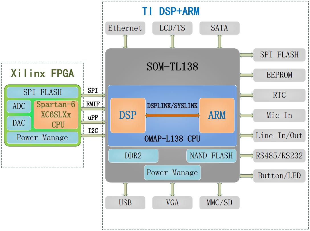
Figure 1 OMAP-L138+FPGA Triple-Core High-Speed Data Acquisition and Processing Resource Block Diagram
Framework Analysis:
The front-end, consisting of a Xilinx Spartan-6 XC6SLX9/16/25/45 FPGA, acquires two channels of AD data with a sampling rate of up to 65MHz. The AD data is transmitted to the OMAP-L138's DSP via uPP or EMIF bus. After being processed by the DSP, the AD data is sent to the ARM via DSPLINK or SYSLINK dual-core communication components for application interface development, network forwarding, SATA hard drive storage, and other applications. The OMAP-L138's DSP or ARM sends the resulting logic control commands to the