Hardware-Software Co-design Architecture for Zynq-based Object Detection Systems (Part 1)
In today's rapidly advancing era of artificial intelligence, object detection has emerged as a crucial task in the field of computer vision, profoundly transforming human society's production and lifestyle. From environmental perception in autonomous vehicles [1, 2] to defect recognition in industrial quality inspection [3, 4], from surface monitoring in satellite remote sensing [5, 6] to lesion analysis in medical imaging [7], object detection technology has become a vital engine driving the development of artificial intelligence.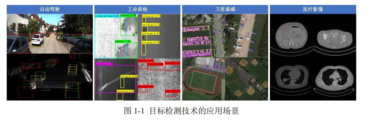
However, with the evolution of deep learning technology, object detection algorithms based on Convolutional Neural Networks (CNNs) have shown an exponential increase in network layers, making their computational processes increasingly complex and their parameters exceeding tens of millions. While an increase in network layers improves model detection accuracy to some extent, it poses severe challenges to the computational and storage resources of hardware platforms. This contradiction between algorithmic complexity and hardware performance is particularly prominent in low-power, real-time scenarios such as industrial inspection and in-vehicle systems. To address this challenge, researchers must not only focus on optimizing network architectures but also explore effective solutions in the hardware domain.
Traditional CPU platforms, as core processors, are limited by their serial architecture design and cannot meet the parallelization demands of dense matrix operations in convolutional neural networks, making it difficult to improve computational efficiency. Currently, Graphics Processing Units (GPUs), Application-Specific Integrated Circuits (ASICs), and Field-Programmable Gate Arrays (FPGAs) are the main platforms used to deploy and accelerate neural networks [8]. GPUs, with their massive parallel computing units, demonstrate significant advantages during the deep learning training phase and are a common choice for accelerating convolutional neural networks [9-11]. However, because GPUs primarily aim for high-performance computing, their power consumption and heat dissipation requirements increase accordingly, often resulting in larger physical sizes. Therefore, in embedded systems, high-temperature environments, or scenarios with strict power consumption requirements, the high power consumption and larger size of GPUs can lead to deployment difficulties and overheating risks. ASICs achieve a high degree of algorithm-hardware matching through customized design [12-14], exhibiting excellent energy efficiency and inference speed. However, due to their highly customized nature, their flexibility is extremely low; once an algorithm iterates or an application scenario changes, the chip requires re-taping, leading to long development cycles and high costs.
The hardware design of object detection systems must balance control flexibility with computational performance, meeting the real-time requirements of traditional embedded applications while providing hardware acceleration capabilities for complex algorithms. The Zynq platform, with its advantages in heterogeneous computing architecture and high-speed data transfer technology, can meet these demands. The overall system hardware architecture design adopts a "top-down" approach, starting with hardware-software co-design for functional partitioning and data flow, and then implementing the design of each module in the PS (Processing System) and PL (Programmable Logic) sides separately.
3.1 Zynq Platform Architecture and Key Technologies
3.1.1 Introduction to the Zynq Platform
Zynq is a Xilinx-developed All Programmable System-on-Chip (SoC) that integrates an ARM processor with an FPGA on the same chip, interconnected via AXI buses, enabling hardware-software co-design [67]. Its structural diagram is shown in Figure 3-1.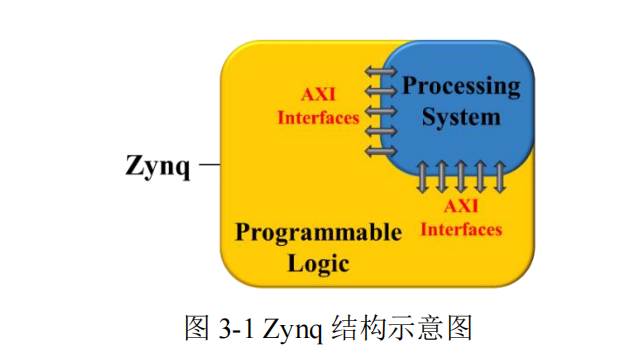
3.2.2 System-Level Architecture Implementation and Control Flow Design
Based on the task partitioning strategy, the overall system framework is built as shown in Figure 3-6.
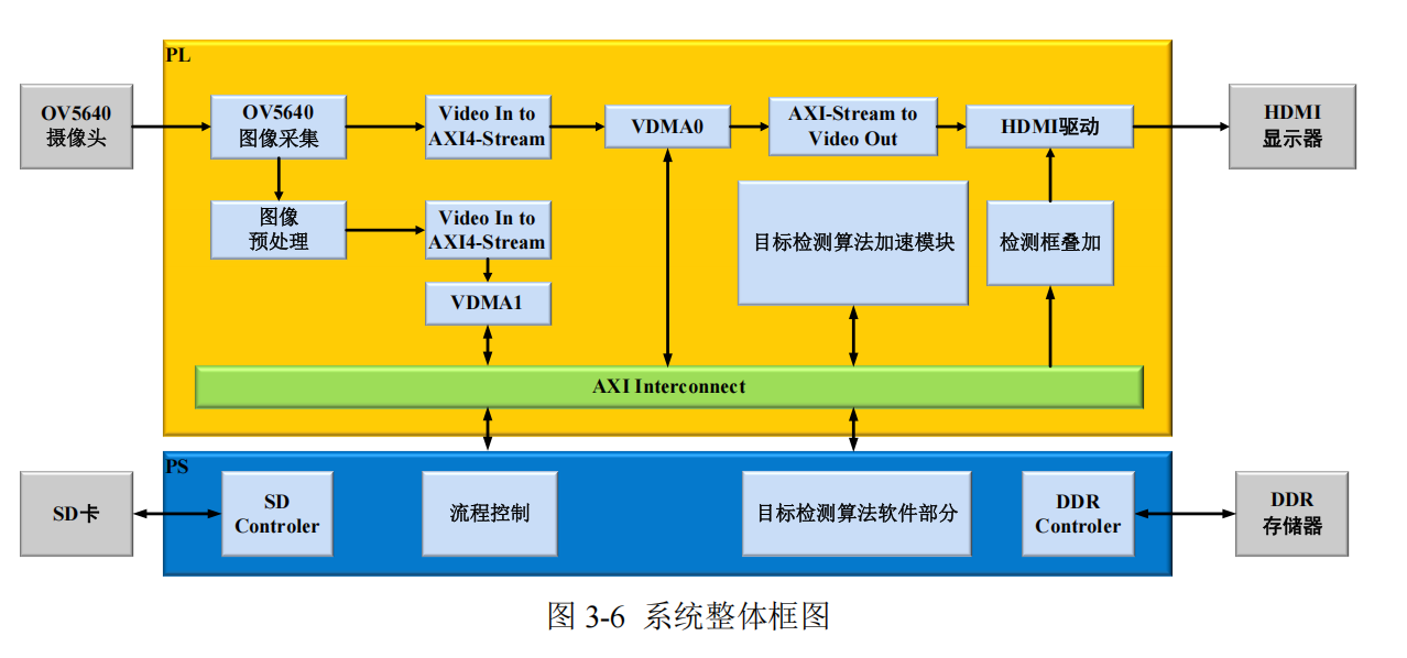
The actual control flow is as follows:
(1) Initialization Phase After the Zynq embedded development board powers on, the PS side loads the trained object detection model's weights and bias parameters from the SD card into DDR memory, preparing the data for subsequent computations.
(2) Image Acquisition The OV5640 image acquisition module initializes the OV5640 and drives it to collect image data as the system input. The data is then saved to DDR memory via VDMA0.
(3) Image Preprocessing The image preprocessing module primarily performs downsampling on the images acquired by the camera, compressing them to 416×416. This data is then transferred to DDR via VDMA1 to serve as input for the object detection model.
(4) Object Detection Algorithm Forward Inference Computation The preprocessed image data is input into the object detection algorithm acceleration module via VDMA1 for inference. The PS side controls the computation flow, and the object detection algorithm acceleration module in the PL side completes computations such as convolution and pooling for each layer.
(5) Object Detection Algorithm Post-processing Computation On the PS side, the feature maps output by the object detection algorithm acceleration module are first processed and decoded into bounding box coordinates, confidence scores, and class information. Subsequently, Non-Maximum Suppression (NMS) is applied to eliminate redundant detection boxes, retaining only the most probable detection results for each object. Finally, the coordinates of these detected bounding boxes are remapped back to the original image.
(6) Detection Result Output The detection results are saved back to the SD card for subsequent processing on a PC. The bounding box overlay module transmits the bounding box coordinates to the HDMI driver module, and the results are finally output on a monitor via HDMI. This completes one detection cycle, and the system prepares for the next.
3.3 PS Side Module Design
The PS side, as the control core of the system, undertakes global task scheduling, data management, and complex logic processing functions. Its design revolves around three core modules: system flow control, image stitching optimization, and object detection post-processing, achieving efficient inference and resource optimization through hardware-software co-design.
3.3.1 System Data and Flow Control
In the system architecture, the PS side bears the important responsibility of hardware system data and flow management. The system's data flow and control flow are transmitted separately through their respective independent interfaces, as shown in Figure 3-8. The PS side controls the PL side components via the M_AXI_HPM0_LPD interface, which connects to various modules within the FPGA through an AXI Interconnect. This interface is primarily used to control data flow within the FPGA and interactions between modules. It can control data transfer between VDMA0, VDMA1, the object detection algorithm acceleration module, and others, coordinating their data processing and transmission order. Concurrently, it connects to AXI4_Lite_box, transmitting relevant control information to the bounding box coordinate transfer module via this interface, ensuring that bounding box coordinates and other information are transmitted and processed according to the correct flow. For data interaction, the PS side primarily uses the S_AXI_HP interface for high-speed data transfer with VDMA0, VDMA1, and the object detection algorithm acceleration module in the PL side.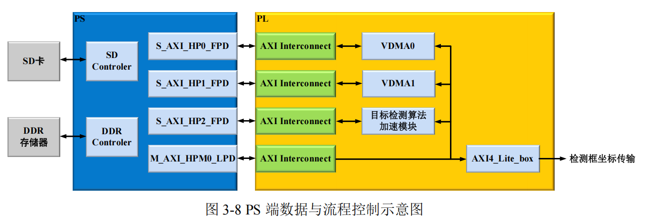
3.3.2 Image Stitching
In the YOLOv4-tiny model, the concat layer appears in Resblock_Body and FPN, totaling 7 operations. The function of this layer is to stitch feature maps from two different levels, preserving the spatial structural information of each feature map while superimposing more semantic information to achieve multi-scale information fusion, thereby improving detection performance. In this design, the PS side is responsible for implementing this part of the operation. The PS side does not need to read stored data for processing; it only needs to calculate offsets when the PL side requests to cache data for stitching and copy the data from each input feature map into the target array in channel order to complete image stitching.
3.3.3 Object Detection Post-processing
Object detection post-processing is the core process of converting feature maps output by a neural network into final detection results, as shown in Figure 3-9, and primarily includes the following modules:
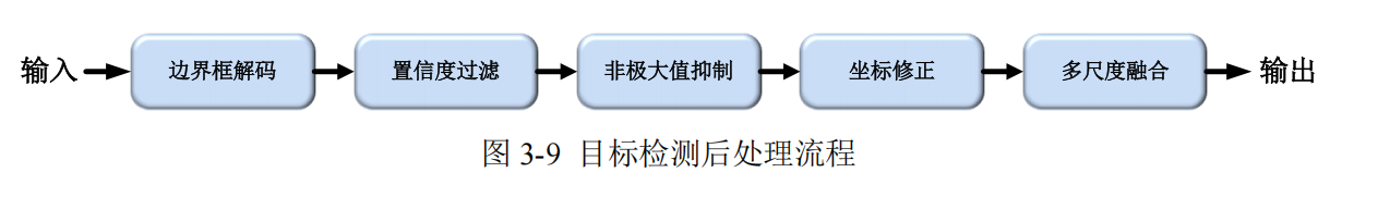
(1) Bounding Box Decoding: Maps the coordinate offsets from the feature map to the original image space, completing geometric transformations using preset anchor parameters.
(2) Confidence Filtering: Eliminates low-quality candidate boxes through thresholding, retaining prediction results with confidence > 0.5.
(3) Non-Maximum Suppression (NMS): IoU-based elimination of overlapping boxes, employing a class-aware iterative suppression strategy.
(4) Coordinate Correction: Maps normalized coordinates to the original image resolution and performs boundary cropping to prevent out-of-bounds issues.
(5) Multi-scale Fusion: