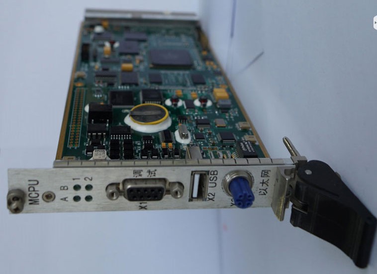
MPC8377-based MCPU 3U CPCI Board
This post covers the hardware architecture and specifications of an MPC8377-based Master Control Processing Unit (MCPU) designed in the 3U CompactPCI form factor. Boards like this occupy a critical role in industrial control systems — bridging the gap between field-level I/O and supervisory software by handling logic execution, inter-board communication, safety switching, and persistent data storage in a single ruggedized module.
Board Role in a CPCI Chassis
The MCPU is the brain of a CompactPCI (CPCI) rack system. In a typical industrial deployment, peripheral boards — analog I/O, digital I/O, communication front-ends — plug into the same passive backplane and exchange data with the MCPU over the CPCI bus. The MCPU is responsible for:
- Logic control — executing control algorithms, ladder logic, or function-block programs that determine actuator outputs from sensor inputs
- Data processing — filtering, scaling, and aggregating raw measurements before they are acted upon or logged
- Communication management — arbitrating traffic between the backplane and external host systems or HMIs over serial and Ethernet interfaces
- System safety protection switching — monitoring watchdog signals and triggering safe-state transitions if a fault is detected
- Data storage — retaining configuration, calibration, and event logs across power cycles using non-volatile memory
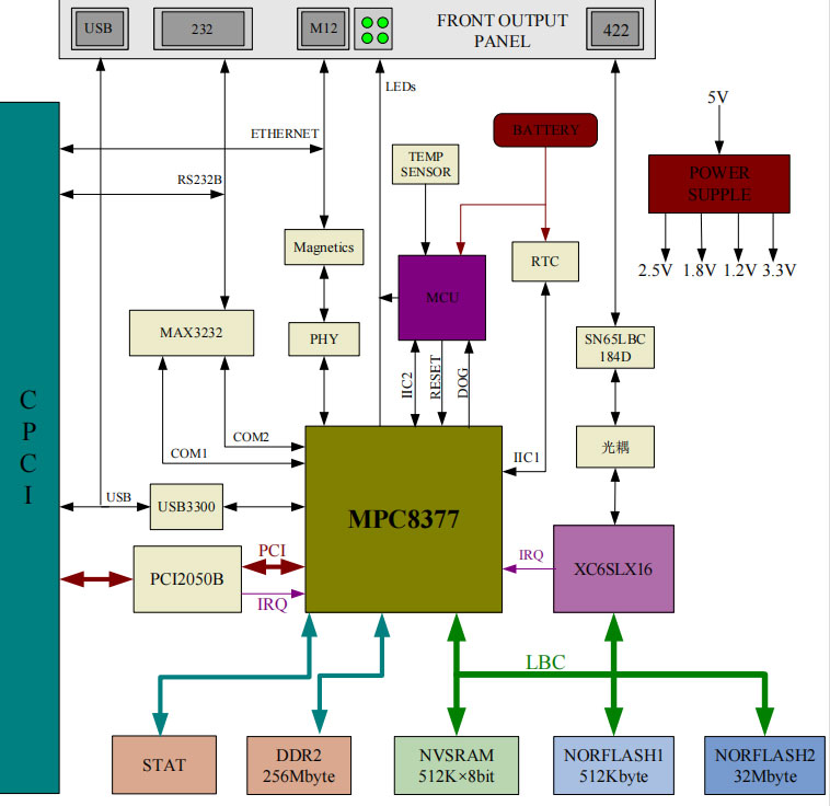
Processor and Core Architecture
The board is built around the Freescale MPC8377, a member of the PowerQUICC II Pro family. This is a single-core, 32-bit Power Architecture processor running at 667 MHz. The PowerQUICC II Pro line was widely adopted in industrial and telecommunications equipment because it integrates a rich set of on-chip peripherals — Ethernet MACs, USB, PCI controller, UARTs, and DMA engines — reducing the need for discrete glue logic on the PCB. At 667 MHz with a 32-bit datapath, the MPC8377 delivers adequate deterministic throughput for real-time control loops while remaining well within the power budget of a DC 5 V board.
Co-Processors: MCU and FPGA
Alongside the main CPU, the board carries two additional programmable devices that handle tasks where the MPC8377's software overhead would introduce unacceptable latency or timing jitter.
MCU — MK60DN512VLL10: This is a Kinetis K60 microcontroller from NXP (originally Freescale), an ARM Cortex-M4 core with 512 KB of on-chip flash and hardware floating-point. In MCPU boards of this class, the MCU typically manages low-level safety watchdog functions, power sequencing, and fast discrete I/O that must respond in microseconds regardless of what the main CPU is doing.
FPGA — XC6SLX16-2FT256I: This is a Xilinx Spartan-6 device in the FT256 package (256-ball fine-pitch BGA), speed grade -2, industrial temperature range (-40 °C to +100 °C). With approximately 14,579 logic cells, the LX16 is mid-range in the Spartan-6 family — large enough to implement custom communication protocols, parallel bus bridges, or real-time signal processing pipelines, yet compact enough to fit on a 3U card with a controlled power budget. The industrial temperature suffix is significant: it guarantees the device meets timing specifications across the full -25 °C to 70 °C operating envelope claimed by the board.
Memory Subsystem
The memory architecture is deliberately segmented to serve the different access patterns of the CPU and FPGA:
| Memory | Size | Users | Purpose |
|---|---|---|---|
| DDR2 SDRAM | 256 Mb (32 MB) | CPU only | Main program execution, OS heap, data buffers |
| PROM | 16 MB | FPGA only | FPGA bitstream storage and configuration |
| NVSRAM | 512 KB | CPU + FPGA (shared) | Retentive variables, event logs, safety state |
| NORFLASH1 | 512 Kb (64 KB) | CPU + FPGA (shared) | Boot parameters or small shared tables |
| NORFLASH2 | 32 Mb (4 MB) | CPU + FPGA (shared) | Firmware images, larger configuration blobs |
The dual-port NVSRAM deserves particular attention. NVSRAM (Non-Volatile SRAM) combines SRAM access speed with battery-backed or capacitor-backed retention, making it the go-to choice for data that must survive a power interruption without the erase-before-write latency penalty of flash. Sharing it between the CPU and FPGA allows the two devices to exchange state — for example, the FPGA can write a fault code into NVSRAM and the CPU can read it at boot time to determine why the previous cycle ended unexpectedly.
Communication Interfaces
Front Panel (Operator/Maintenance Access)
- USB × 1 (USB-A): Typically used for firmware updates, log extraction, or connecting a USB-to-serial adapter during commissioning.
- RS-422 × 1 (D-SUB 9): RS-422 is a balanced differential serial standard supporting cable runs up to several hundred metres and data rates up to 10 Mbps. It is commonly used to interface with encoders, PLCs, or legacy instruments in noisy industrial environments.
- RS-232 × 1 (D-SUB 9): Standard async serial for local debug consoles, HMI panels, or low-speed instrument interfaces.
- Ethernet × 1 (M12-D coded): The M12-D connector is an IP67-rated circular connector widely used in industrial Ethernet applications where vibration or liquid ingress rules out standard RJ-45. This port provides network connectivity to SCADA systems, engineering workstations, or plant-floor networks.
Backplane (System Integration)
The backplane interface is the CPCI bus — CompactPCI, defined by PICMG 2.0. CPCI uses the PCI electrical and logical specification on a Eurocard mechanical form factor with 2 mm hard-metric connectors. The 3U height means the board occupies three rack units in the vertical dimension, giving it a 100 mm board height. The 32-bit/33 MHz CPCI bus delivers up to 133 MB/s of theoretical bandwidth between cards in the chassis, more than sufficient for the inter-board communication typical in control applications.
Physical and Environmental Characteristics
| Parameter | Value |
|---|---|
| Board dimensions | 220 mm × 100 mm × 1.6 mm |
| Weight | 160 g |
| Supply voltage | DC 5 V |
| Operating temperature | -25 °C to +70 °C |
The 220 × 100 mm footprint is standard for 3U Eurocard form factor. The 1.6 mm PCB thickness is the IPC industry standard for this card size, balancing rigidity against weight. At 160 g, the board is light enough that standard CPCI card guides and ejector handles can manage the mechanical load without additional retention hardware.
The -25 °C to +70 °C operating range, combined with the industrial-grade FPGA and the sealed M12 Ethernet connector, positions this board for deployment in outdoor cabinets, rolling stock, or factory floors where temperature excursions and vibration are routine.
Functional Block Diagram
Summary
The MPC8377-based MCPU 3U CPCI board is a well-balanced industrial compute module: a deterministic 667 MHz PowerPC core handles the control loop and system software, an ARM Cortex-M4 MCU takes on safety-critical low-latency tasks, and a Spartan-6 FPGA provides flexible hardware acceleration and custom I/O. The shared NVSRAM and NORFLASH architecture ensures that state can be exchanged between the CPU and FPGA without software overhead, and that critical data persists through unexpected power loss. Combined with industrial-grade connectors, a wide temperature range, and a standard CPCI backplane interface, this board is a capable building block for rail, energy, or factory automation systems that demand long service lives and deterministic control behaviour.