Design of an ARM+FPGA-based Multi-channel Ultrasonic Signal Acquisition and Transmission System
Addressing the challenges faced by ultrasonic signal acquisition systems in multi-channel synchronous acquisition and high-speed data transmission, an 8-channel ultrasonic signal synchronous acquisition and transmission system based on FPGA was designed and implemented. The system uses an FPGA as the main control chip, ADI's AD9279 as the analog front-end and analog-to-digital converter chip for 8-channel ultrasonic signal synchronous acquisition, and achieves data buffering and high-speed data transmission via DDR3 SDRAM and USB 3.0. Experimental results show that the system performs well in multi-channel ultrasonic signal synchronous acquisition, data buffering, and high-speed data transmission, providing a reliable hardware platform for synchronous acquisition and high-speed transmission of multi-channel ultrasonic signals.
0 Introduction
In recent years, ultrasonic testing technology has been widely applied in fields such as medical diagnosis, industrial non-destructive testing, and underwater exploration [1]. Particularly in the medical field, ultrasonic testing has become a common method for disease diagnosis due to its non-invasive, real-time, and safe advantages. However, ultrasonic signals are often weak in practical applications, especially in deep tissues or complex structures, where signal strength can significantly decrease [2]. To extract effective information from weak ultrasonic signals, the precision and accuracy requirements for ultrasonic testing systems are continuously increasing. In this process, the application of array sensors, i.e., multi-channel synchronous ultrasonic testing, has become key to improving system performance. Among these, synchronous acquisition and transmission of multi-channel ultrasonic signals are at the core of ultrasonic testing, with acquisition synchronicity and data transmission speed directly affecting detection accuracy and reliability. Traditional data acquisition and transmission systems typically use microcontrollers and DSPs as main control chips to manage ADCs, memory, host computer communication devices, and other peripheral circuits for data acquisition and transmission. However, traditional processor architectures are prone to delays, instability, or insufficient resources when processing high-speed parallel data, and struggle to balance the real-time and synchronous requirements of acquisition and transmission, thus failing to meet the demands for multi-channel ultrasonic signal synchronous acquisition and high-speed transmission [3-5]. Therefore, Field Programmable Gate Arrays (FPGAs), with their high-speed parallel processing capabilities, have gradually become the main control chips in ultrasonic testing systems. For example, Wang Xiaochun et al. [6] designed an FPGA-based dual-channel high-frequency medical ultrasonic signal synchronous acquisition and transmission system, using First-In, First-Out (FIFO) data buffers for data caching and transmitting data to a host computer via a USB interface for subsequent processing. Sun Tian et al. [7] used an FPGA to control the sequential switching of analog switches and ADC channels, achieving a 4-channel pseudo-synchronous data acquisition scheme and transmitting data via an Ethernet interface. Zhu Zimeng et al. [8] designed a multi-source data acquisition system based on AD7606, achieving 8-channel parallel acquisition at a 100kHz sampling rate and transmitting data via USB 2.0, but without considering a data buffering module. In the 4-channel ultrasonic signal acquisition system developed by Savoia et al. [9], the FPGA's built-in embedded Random Access Memory (RAM) was used to buffer ultrasonic data, ensuring the accuracy of acquired data.
To achieve higher precision, accuracy, and data rates for multi-channel ultrasonic signal synchronous acquisition and transmission, this paper designs an 8-channel ultrasonic signal synchronous acquisition and transmission system based on FPGA.
1 Hardware Design Scheme
1.1 Overall System Design
The 8-channel ultrasonic signal synchronous acquisition and transmission system primarily consists of three parts: the FPGA control module, the signal acquisition module, and the data transmission module. The overall system design is shown in Figure 1.
Figure 1 Overall System Design
The 8-channel ultrasonic signals are first processed by the analog front-end in the AD9279 evaluation board. The FPGA adjusts the gain of the Variable Gain Amplifier (VGA), Low Noise Amplifier (LNA), and Anti-Aliasing Filter (AAF). The A/D converter performs analog-to-digital conversion on the processed analog signals, and the converted digital signals are cached in DDR3 SDRAM, completing the acquisition of ultrasonic data. During USB 3.0 data transmission, the host computer software sends a read data command, transmitting the signals buffered in DDR3 to the host computer via the USB interface. Finally, the data is displayed on the host computer and saved as a .txt file.
1.2 FPGA Control Module
The main control board of the system described in this paper uses a development board based on Xilinx Artix-7 series FPGA chips, model XC7A100T [10]. This development board features a compact and exquisite design, roughly the size of a standard credit card. The core board of this development board uses a 100 MHz active crystal oscillator as the system clock. It also integrates two high-speed 512MB DDR3 SDRAM memory chips [11] for buffering ultrasonic signals. A USB 3.0-based communication interface is used for data interaction with the host computer and simultaneously powers the board. Board-to-board connectors provide expansion interfaces, offering adjustable voltage levels of 3.3V/2.5V/1.8V and differential routing, which perfectly meets the design requirements of this paper.
1.3 Signal Acquisition Module
1.3.1 AD9279 Evaluation Board
In the process of ultrasonic signal acquisition, the Analog Front-End (AFE) and Analog-to-Digital Converter (ADC) are two of the most critical modules. After signals are acquired from the transducer via AC coupling, the AFE receives and pre-processes the analog ultrasonic signals, and the ADC converts the analog signals output by the AFE into digital signals [12]. Considering factors such as acquisition precision, synchronicity, number of channels, and cost, this system adopts the AD9279, a high-speed integrated analog front-end module manufactured by ADI. Processes such as ultrasonic signal amplification, filtering, analog-to-digital conversion, and Low-Voltage Differential Signaling (LVDS) serial transmission are all implemented within the AD9279. The AD9279 supports 8-channel synchronous acquisition and integrates an 8-channel Variable Gain Amplifier, Low Noise Preamplifier, Anti-Aliasing Filter, 12-bit 80 MSPS Analog-to-Digital Converter, and a programmable phase rotation I/Q demodulator [13]. This allows for precise timing synchronization across all eight channels. By configuring registers via the Serial Peripheral Interface (SPI), the gain coefficients of each channel can be controlled, ensuring the synchronicity and reliability of 8-channel ultrasonic signal acquisition.
1.3.2 AD9279 FPGA Interconnect Board Hardware Design
After the ADC converts analog signals into digital signals, the digital signals need to be transmitted to the FPGA for further processing.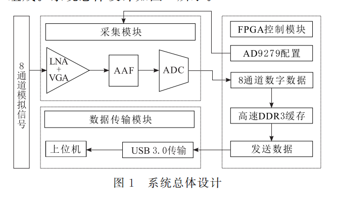 In this process, the most critical issue is how to connect the AD9279 evaluation board to the FPGA development board to ensure correct transmission of the converted ultrasonic digital signals to the FPGA for subsequent processing.
3 Experimental Results
First, the 8-channel synchronous data acquisition function was verified, with the verification experiments shown in Figures 8 and 9.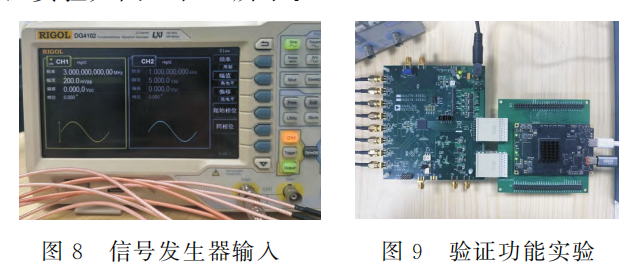
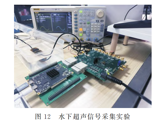
Finally, an underwater ultrasonic acquisition experiment was conducted to verify the system's actual capability to acquire ultrasonic signals. As shown in Figure 12, two ultrasonic transducers were placed in a water medium. A signal generator produced a sine wave signal with a peak-to-peak voltage (Vpp) of 1V and a frequency (f) of 3.5MHz, which was connected to transducer A. Transducer A emitted ultrasonic signals, and transducer B converted the received ultrasonic signals into analog voltage signals, which were then input into channel 1 of the AD9279. Finally, the acquired ultrasonic signals were transmitted to the host computer for reconstruction.
Figure 12 Underwater Ultrasonic Signal Acquisition Experiment
The reconstructed ultrasonic acquisition signal is shown in Figure 13. It can be seen that the signal is complete with no obvious distortion, indicating that the system has excellent capability for acquiring ultrasonic signals.
Sienovo supports ARM+FPGA+AD customization.