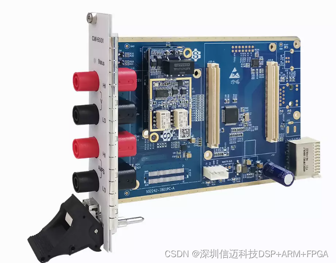
Plug-in Instrument Module: Digital Multimeter Module (Plug-in Type)
Plug-in instrument modules bring the precision of bench-top test equipment directly into embedded and FPGA-based data acquisition systems. This post covers the specification details of a plug-in digital multimeter (DMM) module, explaining what each parameter means in practice and how engineers can use this module for high-accuracy electrical measurement across voltage, current, resistance, inductance, and capacitance.
What Is a Plug-in DMM Module?
Unlike stand-alone benchtop multimeters, plug-in DMM modules are designed to seat into a chassis backplane — common in PXI, CompactDAQ, or proprietary modular instrument systems. This form factor lets you combine multiple measurement channels into a single controlled environment, synchronize acquisitions across modules, and automate test sequences without manual probe intervention. The module described here offers a 6½-digit display equivalent, meaning it can resolve readings to seven significant digits in display terms — on par with mid-range bench instruments.
Key Specifications at a Glance
The module's headline figures are worth unpacking before diving into the channel-level detail:
- 6½-digit display — resolves up to 1,999,999 counts, giving sub-ppm readability on most ranges.
- 24-bit ADC resolution — the underlying converter provides approximately 16.7 million discrete levels, well beyond what the display shows, allowing software averaging and noise analysis.
- 250 KSPS sampling rate — 250,000 samples per second, which is high for a precision DMM (many lab instruments sample far slower to prioritize noise rejection). This rate enables time-domain transient capture alongside DC accuracy.
- Isolated power supply and digital I/O — galvanic isolation prevents ground loops from corrupting measurements and protects both the DUT and the host system from common-mode voltages.
Channel Configuration
The module offers three channels arranged across two physical connectors:
| Channel 1 | Channel 2 | Channel 3 | |
|---|---|---|---|
| Input Impedance (Voltage) | 10 MΩ | High-Z, 10 MΩ | — |
| Input Impedance (Current) | 10 Ω | 50 mΩ / 2 Ω / 2 KΩ | — |
| Voltage Range | ±5 V | 0–60 V | — |
| Current Range | ±2 mA | 1 nA – 3 A | — |
| Resistance Range | — | 1 MΩ – 100 MΩ | — |
| Coupling | DC | DC | DC |
| ADC Resolution | 24 bits | 24 bits | 24 bits |
| Sampling Rate | 250 KSPS | 250 KSPS | 250 KSPS |
Channel 1 is oriented toward low-level bipolar voltage and small current signals (±5 V / ±2 mA), making it suitable for sensor output monitoring, op-amp circuit verification, and low-power device characterization. Channel 2 covers the wider voltage range (0–60 V) and spans a much broader current window (1 nA to 3 A), with selectable shunt resistances (50 mΩ, 2 Ω, or 2 KΩ) that trade off sensitivity against burden voltage across the current path.
Measurement Accuracy — Reading the Spec
DMM accuracy specs always follow the format ± (X% of Reading + Y% of F.S.), where:
- % of Reading is a gain error — it scales with the measured value.
- % of F.S. (full scale) is an offset error — it is fixed regardless of the reading.
Understanding both terms matters: at small readings near zero, the F.S. term dominates; at readings near full scale, the Reading term becomes more significant.
Voltage
Channel 1 (±5 V range):
± (0.018% of Reading + 0.0015% of F.S.)
This is an excellent DC voltage spec. At a 5 V full-scale reading, the combined worst-case error is approximately ±1.65 mV — suitable for precision reference verification and ADC calibration tasks.
Channel 2 voltage accuracy varies by sub-range:
| Sub-range | Accuracy |
|---|---|
| 6 mVDC | ± (0.06% of Reading + 0.075% of F.S.) |
| 6 VDC | ± (0.018% of Reading + 0.0013% of F.S.) |
| 60 VDC | ± (0.03% of Reading + 0.001% of F.S.) |
| 6 VAC | ± (1% of Reading + 0.1% of F.S.) |
The AC voltage accuracy (±1% of Reading) is notably looser than DC — expected behavior, since AC measurement requires RMS conversion and is frequency-dependent. For AC signals above a few kilohertz, verify the module's AC bandwidth before relying on these figures.
Current
Channel 1 (±2 mA range):
± (0.06% of Reading + 0.06% of F.S.)
Channel 2 current accuracy scales with the shunt resistor selected:
| Sub-range | Accuracy |
|---|---|
| 1 µADC | ± (0.1% of Reading + 0.1% of F.S.) |
| 100 mADC | ± (0.05% of Reading + 0.02% of F.S.) |
| 3 ADC | ± (0.1% of Reading + 0.02% of F.S.) |
The nano-amp range (1 nA–1 µA implied by the 1 µADC sub-range) demands careful attention to cable leakage, PCB surface resistance, and guard routing. At these levels, even a few hundred megaohms of parasitic leakage path can corrupt readings.
Resistance
| Range | Accuracy |
|---|---|
| 1 Ω | ± (1% of Reading + 0.1% of F.S.) |
| 100 Ω | ± (0.05% of Reading + 0.2% of F.S.) |
| 1 MΩ | ± (0.05% of Reading + 0.006% of F.S.) |
| 100 MΩ | ± (0.9% of Reading + 0.01% of F.S.) |
Resistance accuracy degrades at both extremes of the range — the 1 Ω spec carries a 1% Reading error because lead and contact resistance become significant fractions of the measured value. For sub-ohm measurements, a four-wire (Kelvin) connection is strongly recommended to eliminate lead resistance from the measurement loop. At the high end (100 MΩ), the 0.9% Reading error reflects the challenges of sourcing a stable, low-leakage test current across a high-impedance path.
Capacitance
| Range | Accuracy |
|---|---|
| 1 nF | ± (3% of Reading + 0.5% of F.S.) |
| 1 µF | ± (2% of Reading + 0.1% of F.S.) |
| 500 µF | ± (8% of Reading + 0.5% of F.S.) |
Capacitance measurement is inherently less precise than DC voltage or resistance — the 8% figure at 500 µF is normal for instruments relying on charge/time methods. For high-capacitance electrolytics, account for ESR and self-resonance if the test frequency is not specified by the application. Dedicated LCR meters are preferable when capacitance accuracy below 1% is required.
Diode and Transistor Testing
Beyond passive component measurement, the module supports diode and transistor (BJT) testing. Diode test mode applies a small forward current and reports the forward voltage drop — typically 0.6–0.7 V for silicon, 0.2–0.3 V for Schottky, and near-zero for a shorted junction. Transistor test mode (hFE measurement) applies a base current and measures collector current to derive DC current gain. These modes are useful for incoming inspection and board-level fault isolation without needing a separate component tester.
Integration Considerations
With 24-bit resolution and 250 KSPS throughput, this module is well-suited for applications that need both static precision and dynamic capture in a single instrument:
- Production test — rapid automated parametric measurement of assembled PCBs.
- Power supply characterization — capturing load transients at 250 KSPS while maintaining sub-millivolt DC accuracy.
- Sensor calibration — high-Z input on Channel 2 avoids loading precision resistive or bridge sensors.
- FPGA-based instrumentation — the isolated digital I/O interface allows direct connection to FPGA front-ends without risk of ground-plane contamination from switching noise.
The isolated power and signal architecture is particularly valuable in industrial environments where ground potential differences between chassis and field wiring can reach several volts — conditions that would saturate or damage non-isolated measurement inputs.