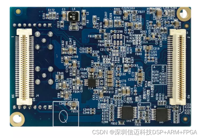
NI Alternative (Domestic): High-Speed Data Acquisition Module with Max Sampling Rate of 125 Msps, Supporting FPGA Customization
For engineers working in test and measurement, industrial automation, or RF signal processing, finding a high-performance data acquisition module that matches the capabilities of National Instruments (NI) hardware — without the NI price tag — has historically been a significant challenge. This post covers a domestically produced alternative: a dual-channel, high-speed data acquisition module featuring a maximum sampling rate of 125 Msps, 12-bit ADC resolution, and an FPGA-based architecture that allows deep hardware customization.
The Case for a Domestic NI Alternative
NI's CompactDAQ and PXI data acquisition platforms are industry workhorses, but their cost and lead times can be prohibitive for mid-scale industrial projects, embedded R&D labs, and academic applications. The module described here targets that gap directly, offering comparable core specifications — high sample rate, respectable resolution, and programmable logic — in a form factor suited for both prototyping and production deployment.
Core Hardware Specifications
The module's acquisition front-end is built around a dual-channel ADC with the following key parameters:
- Maximum sampling rate: 125 Msps (mega-samples per second)
- ADC resolution: 12 bits
- Maximum input voltage range: ±0.9 V
- -3 dB analog bandwidth: 30 MHz
A 12-bit ADC at 125 Msps provides 4,096 discrete amplitude levels sampled at 8 ns intervals. The ±0.9 V full-scale input range is narrower than general-purpose oscilloscope inputs, which makes this module well-suited for RF front-end applications and intermediate-frequency (IF) signal chains where signals have already passed through conditioning stages. The 30 MHz -3 dB bandwidth is consistent with Nyquist theory for a 125 Msps converter — the analog front-end passes signal content up to roughly the Nyquist frequency before anti-aliasing attenuation becomes significant.
For context, 125 Msps with 12-bit depth places this module in the same general category as NI's PXIe-5122 digitizer and similar mid-range acquisition instruments, which are commonly used for communications signal analysis, vibration measurement, and radar IF capture.
FPGA Customization: The Key Differentiator
What elevates this module beyond a fixed-function digitizer is the integrated FPGA, which allows users to implement custom signal processing pipelines directly in programmable logic — close to the ADC output, before any CPU bottleneck.
The practical benefits of this architecture include:
Hardware-accelerated processing. Instead of streaming raw samples to a host CPU for filtering, decimation, or FFT computation, those operations can be offloaded to the FPGA fabric. This dramatically reduces memory bandwidth requirements and latency, and allows deterministic real-time processing that a general-purpose CPU cannot guarantee.
Application-specific logic. Because the FPGA is user-programmable, the same hardware platform can be adapted to fundamentally different use cases:
- Signal processing: FIR/IIR digital filters, decimation chains, envelope detection, or matched filters for radar and sonar.
- Image processing: Line-scan camera data acquisition, frame synchronization, pixel-level preprocessing.
- Communications: Protocol demodulation, clock recovery, framing logic for custom waveforms.
- Instrumentation: Custom trigger logic, multi-board synchronization, timestamping, and histogram accumulation.
Reduced system complexity. In traditional architectures, high-speed ADC data flows through a high-bandwidth interface (e.g., PCIe or USB 3.0) to a host machine that handles all processing. With an FPGA in the loop, processed — and therefore lower-bandwidth — results can be transmitted instead of raw sample streams, enabling the use of simpler host interfaces and smaller storage buffers.
Typical Application Scenarios
Waveform Acquisition
At 125 Msps, the module can digitize analog signals up to approximately 30 MHz with full fidelity. This makes it appropriate for capturing transient waveforms, characterizing analog front-end circuits, or recording repetitive signals for subsequent averaging and analysis. The dual-channel configuration allows simultaneous capture of two independent signal paths — useful for comparing input vs. output, measuring phase relationships between two channels, or acquiring differential signals.
Frequency Domain Analysis
The combination of 125 Msps sample rate and 12-bit resolution provides good dynamic range for FFT-based spectrum analysis. A 12-bit ADC has a theoretical maximum SNR of approximately 74 dB (6.02 × 12 + 1.76 dB), which is sufficient for identifying harmonic distortion products, spurious signals, and broadband noise floors in the 0–30 MHz band. Users can implement FFT engines directly in the FPGA for real-time spectral monitoring, or stream decimated data to a host for offline analysis.
Positioning vs. NI Hardware
The value proposition of this module is straightforward: domestic sourcing, FPGA programmability, and mid-range specifications at a cost point below equivalent NI PXI or CompactDAQ modules. For applications that do not require NI's full LabVIEW ecosystem or its broader instrument portfolio, a standalone FPGA-based DAQ card like this one can be integrated into custom software stacks using vendor-provided HDL IP or raw register-level drivers, giving engineers full control over both the hardware pipeline and the software interface.
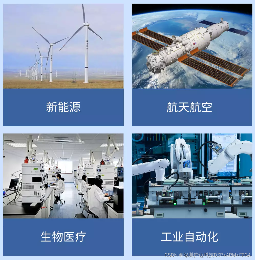
For teams building bespoke test equipment, edge-AI inference pipelines that require sensor digitization, or industrial control systems where supply chain independence is a priority, this class of module represents a practical and technically capable alternative to Western instruments.