Hardware Design of ZYNQ-based Array Eddy Current Testing System (Part 1)
Array eddy current (AEC) testing is a well-established non-destructive evaluation (NDE) technique used to detect surface and near-surface defects in conductive materials. Unlike single-probe eddy current, an array system distributes dozens of drive and sense coils across a probe footprint, enabling rapid C-scan imaging without mechanical raster scanning. Building such a system from scratch demands careful co-design of analog front-end hardware and real-time digital signal processing — a task well suited to a ZYNQ SoC that pairs a hard ARM processor with programmable logic on the same die. This article walks through the hardware architecture of a multi-channel AEC acquisition system built around the Xilinx Zynq-7020, covering the DAC excitation path, power amplifier stage, analog multiplexing, and ADC acquisition chain.
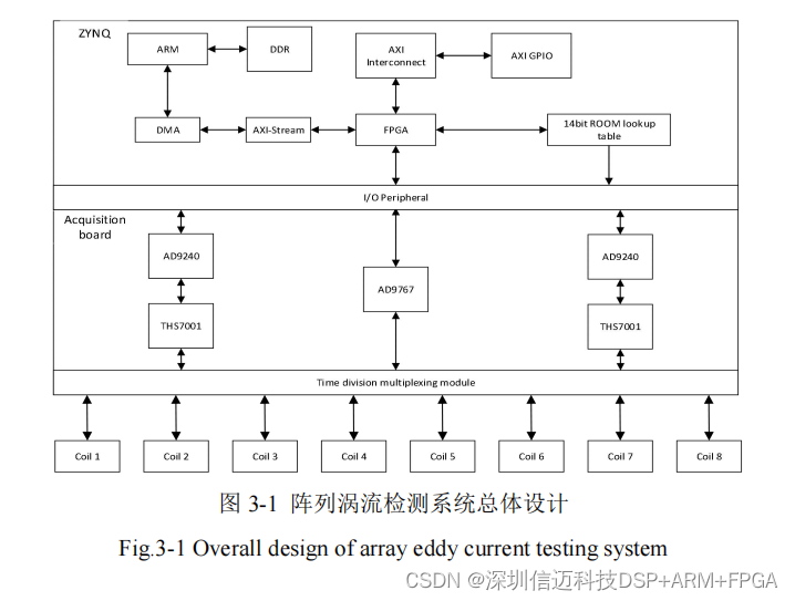
System Architecture Overview
The signal chain follows a classic lock-in topology adapted for multi-channel operation:
- Excitation path — ZYNQ PL reads a sinusoidal lookup table from ROM and streams digital samples to a dual-channel 14-bit DAC. The resulting analog sine wave drives an external power op-amp, which boosts current capacity before feeding the excitation coil through an analog multiplexer.
- Acquisition path — Induced voltages from the sensing coils are digitised by an ADC. The PL buffers samples in a FIFO and runs a digital phase-sensitive detection (PSD) algorithm that decomposes the signal into its real part (resistance component), imaginary part (reactance component), and phase angle.
- Host interface — Processed impedance data is forwarded from the PS (ARM Cortex-A9) to a host PC over Ethernet using the lightweight IP stack (lwIP).
PS and PL communicate over AXI buses using a ping-pong buffering scheme, which keeps data moving without stalling either domain. The PS also hosts the DDR controller, so large acquisition buffers can be staged in DRAM before upload.
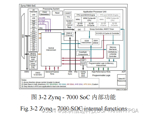
ZYNQ-7020 Platform
The Zynq-7000 family from Xilinx (now AMD) integrates a dual-core ARM Cortex-A9 processing system (PS) with an Artix-7–based programmable logic (PL) fabric on a single chip. The Zynq-7020 specifically offers 85K logic cells, 220 DSP48E1 slices, and 4.9 Mb of block RAM — sufficient to implement parallel FIR filters, the FIFO data path, and a real-time PSD engine simultaneously. Critically for this application, the DSP slices allow the digital lock-in multiplication and accumulation to run at clock rates up to several hundred MHz without consuming soft-logic resources.
The PS–PL boundary is bridged by AXI-HP (high-performance) and AXI-GP (general-purpose) ports. The design uses ping-pong caching across these ports: while the PL writes one buffer with fresh ADC samples, the PS drains the previous buffer over DMA, eliminating pipeline stalls. This architecture is well proven for streaming instrumentation workloads.
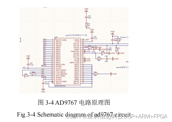
DAC Conversion Circuit — AD9767
The excitation sine wave is generated by reading a pre-computed sinusoidal lookup table stored in PL block RAM and clocking the values into an AD9767 dual-channel, 14-bit CMOS DAC. The AD9767 supports update rates up to 125 MSPS, which is far faster than the kilohertz-range excitation frequencies typical of eddy current testing, giving the design ample headroom for interpolation or multi-tone excitation in future revisions.
Power Supply Pins
- AVDD — analog supply, up to 6.5 V. The AVDD level sets the ceiling of the analog output voltage swing.
- DVDD — digital supply, up to 6.5 V. Raising DVDD above the recommended range increases the threshold the device expects for a valid logic high on the data bus, which can cause data errors if FPGA I/O levels are not matched.
Both supplies should be well-decoupled with ceramic capacitors placed close to the device pins to suppress switching noise from the FPGA logic transitions coupling into the analog output.
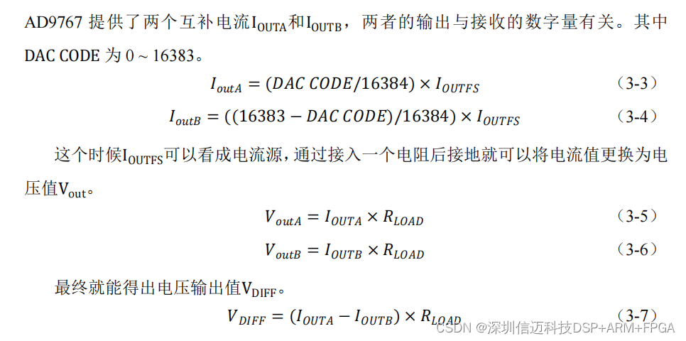
Output Current Scaling
The AD9767 contains an internal control amplifier that sets the full-scale output current I_OUTFS. This current equals 32× the reference current I_REF set by an external resistor on the RSET pin:
I_OUTFS = 32 × I_REF
By constraining I_REF to the range 62.5 µA – 625 µA, I_OUTFS is kept between 2 mA and 20 mA. The output current for a given digital code is:
I_OUT = I_OUTFS × (DAC_CODE / 2^14)
Dual-Port vs. Interleaved Mode
The MODE pin selects between two operating modes:
Dual-port mode (MODE = logic 1, tied to 3.3 V in this design): Each DAC channel has its own fully independent 14-bit data bus, WRT line, and CLK line. Channel 1 uses WRT1/CLK1; Channel 2 uses WRT2/CLK2. The two channels do not interfere with each other. Digital data first latches into an input latch on the rising edge of WRT, then transfers to the DAC latch on the rising edge of CLK, after which the analog output updates. An important PCB timing constraint: CLK must not lag WRT — if CLK is delayed beyond the setup/hold window of the DAC latch, data corruption occurs at the analog output. In practice, WRT and CLK can be tied together so both latches update simultaneously, provided the combined trace lengths are matched.
Interleaved (IQ) mode (MODE = logic 0): WRT1 becomes IQWRT, CLK1 becomes IQCLK, WRT2 becomes IQSEL, and CLK2 becomes IQRESET. On each rising edge of IQWRT the data word enters the device; IQSEL high routes it to channel 1, IQSEL low routes it to channel 2. IQRESET disables IQCLK when high; on the next IQCLK rising edge after IQRESET goes low, the DAC latch updates. This mode is useful for I/Q modulation applications where a single bus alternately feeds both channels, but the added control complexity is unnecessary here.
This design pins MODE high and uses channel 1 only for sinusoidal excitation. Channel 2's 14 data inputs are pulled to ground through 10 kΩ resistors, effectively disabling it while keeping the pins in a defined state.
Differential-to-Single-Ended Conversion — AD8066
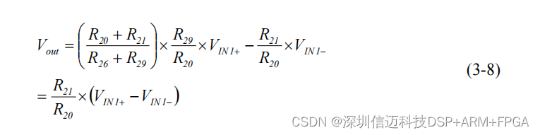
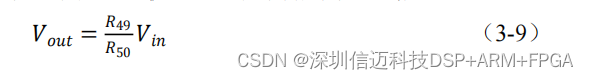
The AD9767 produces complementary current outputs (I_OUT and /I_OUT). A differential-to-single-ended conversion stage using the AD8066 dual voltage-feedback op-amp converts this to a single-ended voltage suitable for the power amplifier input. The AD8066 offers a 145 MHz bandwidth, operates from ±2.5 V to ±12 V (or a single 5 V – 24 V supply), and provides rail-to-rail output — ensuring the full DAC output swing is preserved without clipping. The conversion gain is set by a resistor network (R20, R26, R21, R2) that determines the differential gain and the common-mode rejection.
Power Amplifier Stage — OPA544F
The AD8066 output is a low-current signal — far too weak to drive a copper excitation coil with an inductive load. The OPA544F is a high-voltage, high-current monolithic op-amp capable of sourcing or sinking 2 A continuous output current, making it suitable for driving low-impedance coil loads. Key specifications:
- Supply range: ±10 V to ±35 V (this design uses ±12 V)
- Continuous output current: 2 A
- Internal current limit (thermal protection): 4 A — measured at approximately 3980 mA during reverse-supply stress testing in this design, confirming the protection functions as expected
- Internal thermal shutdown protects against sustained overcurrent conditions
The OPA544F is configured as a non-inverting amplifier powered from ±12 V rails. The gain is set by the feedback resistor divider. Non-inverting configuration is preferred here because it presents high input impedance to the DAC output stage, avoiding loading effects that would distort the sine wave amplitude.
Excitation Channel Analog Switching
To support time-division multiplexed excitation across an array of coils, the power amplifier output must be routed to each coil in sequence. The key constraint when selecting analog switches for this stage is maximum continuous current — most high-integration analog multiplexer ICs are rated for only a few hundred milliamps, which is insufficient for the amp-level currents the OPA544F delivers. After evaluating available options, the design uses one dedicated single-channel analog switch per coil rather than a shared multiplexer, since no single-package multi-channel device with adequate current handling was found. Each switch independently opens or closes its channel, allowing the firmware to activate one coil at a time while keeping all others isolated.
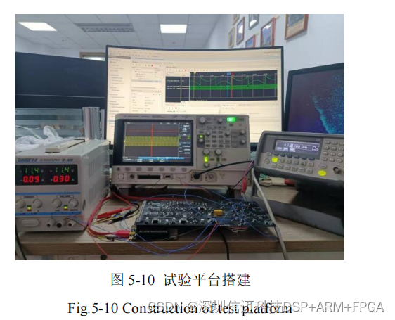
System Validation
The completed hardware — ZYNQ core board, acquisition daughterboard, power supply, and analog front end — was validated using a signal generator as a calibrated reference in place of actual induction coils. A logic analyser captured both the signal generator waveform and the DAC analog output simultaneously, allowing the phase between them to be computed and compared against the phase value produced by the digital PSD algorithm running in PL. Agreement between the hardware-measured phase and the algorithmically computed phase confirms both that the signal chain is operating correctly and that the digital lock-in implementation is numerically accurate.
Part 2 will cover the ADC acquisition circuit, the digital phase-sensitive detection algorithm implemented in VHDL/Verilog, and the lwIP Ethernet data path from PL FIFO to host display.