Zynq+AD+DA-based Vibration Table Controller Architecture Design and Algorithm Implementation - Overall Architecture Design (Part 2)
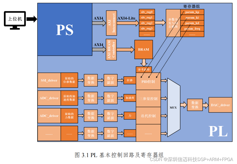
3 Vibration Table Controller Architecture Design and Implementation
As previously mentioned, the Zynq-7000 already possesses unique architectural advantages by combining an ARM Cortex-A9 processor subsystem (PS) with a programmable logic fabric (PL) on a single chip. This tight coupling allows the vibration table controller to partition its workload along a clear boundary: tasks demanding deterministic timing — sampling, filtering, PID computation, and analog output — run entirely in the PL at hardware speed, while tasks that require flexibility but not strict cycle-accuracy, such as host communication and parameter management, run in the PS. This is a critical design distinction. "High-speed" and "real-time" are not synonymous: a USB or Ethernet link may transfer data at hundreds of megabits per second yet tolerate milliseconds of jitter, whereas the control loop must complete within a fixed 1 ms window with no exceptions.
Based on this partitioning principle, the overall program architecture of the Zynq vibration table controller separates PL responsibilities (the closed control loop, ADC/DAC drivers, BRAM buffering) from PS responsibilities (AXI register access, interrupt handling, and upstream communication to the host PC).
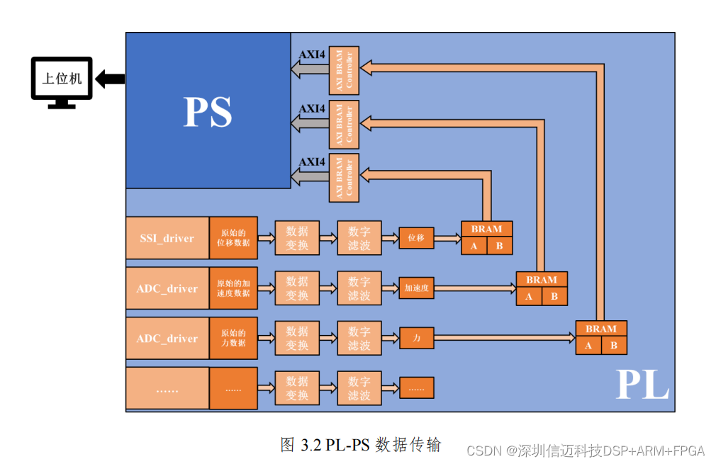
3.1.2 PL-PS Data Transfer
After signal conditioning has been applied to the raw sensor data, both the actual (feedback) signal and the reference signal must be forwarded to the host PC for monitoring and comparison. This requires a reliable, continuous data path from the PL fabric to the PS ARM core.
The chosen approach uses a ping-pong Block RAM scheme:
- PL writes sampled data into BRAM bank A until a target count is reached (for example, 1000 samples).
- Once bank A is full, PL asserts an interrupt to the PS and immediately begins filling bank B.
- PS responds to the interrupt and reads bank A over the AXI bus while PL continues writing to bank B.
- When bank B fills, the roles reverse: PS reads bank B while PL writes bank A.
This alternating read-write pattern guarantees that waveform data flows continuously without gaps or overruns, because neither side ever waits for the other beyond the natural latency of filling one bank. The Verilog logic required to generate the BRAM control signals — write enable, address increment, bank-select toggling, and interrupt generation — is discussed in the key module sections below.
The complete PL-side implementation is shown in Figure 3.3.
3.2 Key PL Module Implementations
The PL-side design encompasses several categories of custom Verilog modules:
| Category | Modules |
|---|---|
| Data acquisition | SSI_driver, AD7606_driver |
| Data processing | Sliding-average filter |
| Data scheduling | BRAM read/write controller |
| SW-HW co-design | Parameter distribution and synchronization |
| Output | DAC81416_driver |
Utility blocks such as AXI Interconnect are generated by Vivado IP integrator; all other modules are hand-written in Verilog. The PL clock runs at 100 MHz, and the main control loop period is 1 ms — meaning the ADC sampling, filter computation, PID update, and DAC output are all completed once per millisecond.
3.2.1 SSI Driver Module
Analog feedback in a vibration control system is inherently noisy. A sensor with a digital output using the SSI (Synchronous Serial Interface) protocol eliminates most of this noise at the source, because SSI was explicitly designed to minimize signal noise over long cable runs using differential signaling (RS-422 levels on Clock± and Data±).
SSI is the most common interface on high-precision absolute encoders. It operates as a synchronous, master-initiated protocol:
- In the idle state, both clock and data lines are held high.
- The master drives the first falling edge of the clock, which causes the encoder to latch its current position and begin shifting out data.
- On each subsequent rising edge, the encoder presents the next bit starting from the MSB.
- After all bits have been transmitted, clock and data return high.
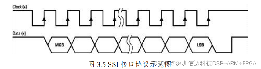
The magnetostrictive linear displacement sensor used in this design outputs 25-bit binary (Gray-code-free Binary) position data. Because the hardware PCB already includes a differential-to-single-ended converter (RS-422 receiver), the FPGA only needs to handle single-ended SSI_clk and SSI_data signals, simplifying the PL interface significantly.
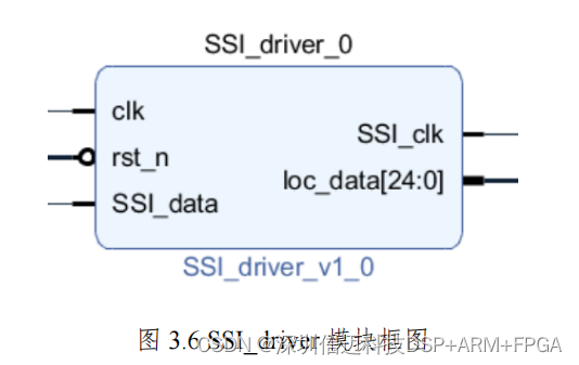
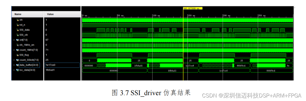
The SSI_driver module block diagram is shown in Figure 3.6, and simulation results confirming correct frame capture are shown in Figure 3.7.
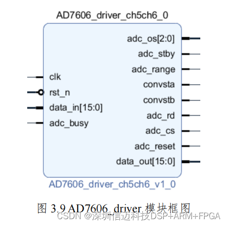
3.2.2 AD7606 ADC Driver Module
The AD7606 (Analog Devices) is an 8-channel, simultaneous-sampling successive-approximation ADC. Key specifications relevant to this design:
- 8 channels sampled simultaneously, eliminating inter-channel phase error
- 16-bit resolution per channel
- Maximum throughput of 200 KSPS per channel
The AD7606 supports several interface configurations; this design selects:
- Parallel output: all 16 data bits transferred simultaneously over a 16-wire bus, with the eight channels read sequentially via chip-select and read pulses
- Post-conversion read: data is read only after the BUSY signal deasserts, confirming that conversion is complete
- Tied CS and RD: the chip-select and read-enable lines are connected together to simplify the control logic
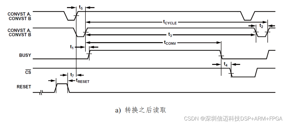
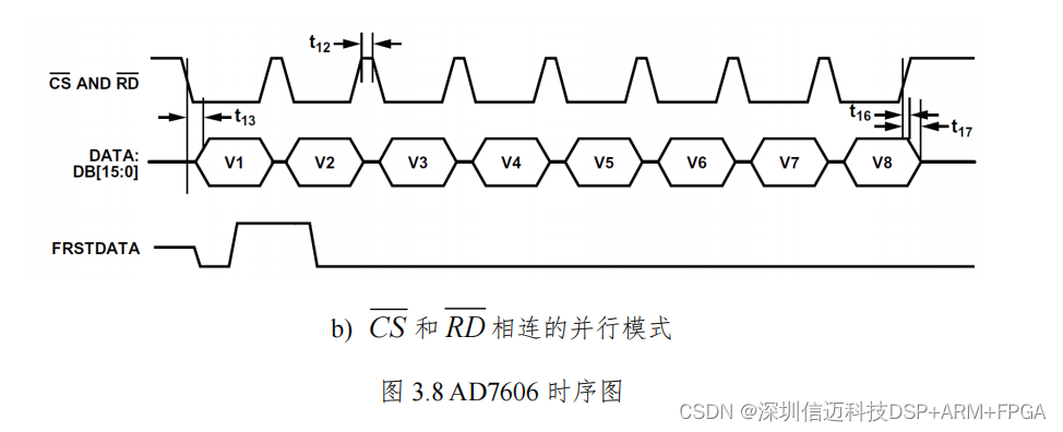
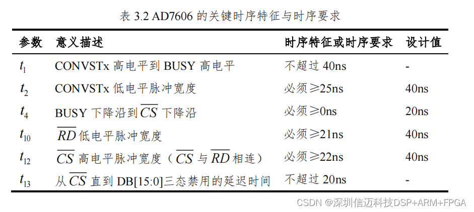
Meeting the AD7606 timing requirements in Verilog requires careful attention to several parameters (see Table 3.2 in the original reference). In particular, detecting the falling edge of the BUSY signal requires pipeline registers (打拍) in the FPGA — registering BUSY through two flip-flop stages before using it for state transitions, which prevents metastability and ensures a clean, synchronous edge-detect.
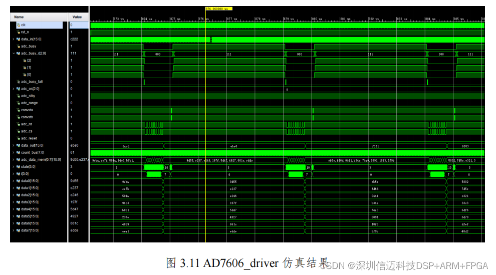
The AD7606_driver state machine runs at the maximum 200 KSPS rate, giving a 5 µs cycle. The state transition diagram (Figure 3.10) sequences through conversion trigger, busy-wait, and sequential channel read states.
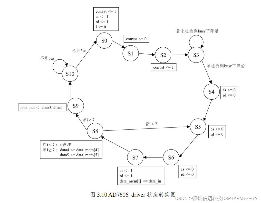
After iterative simulation and timing closure, the AD7606_driver module produces waveforms that satisfy all data-sheet timing constraints.
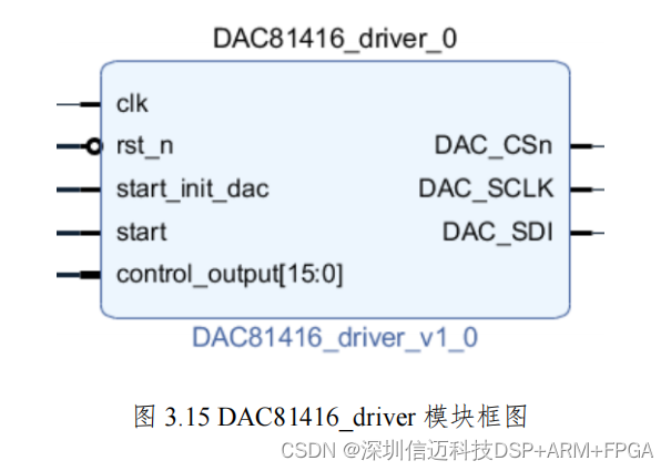
3.2.4 DAC81416 Driver Module
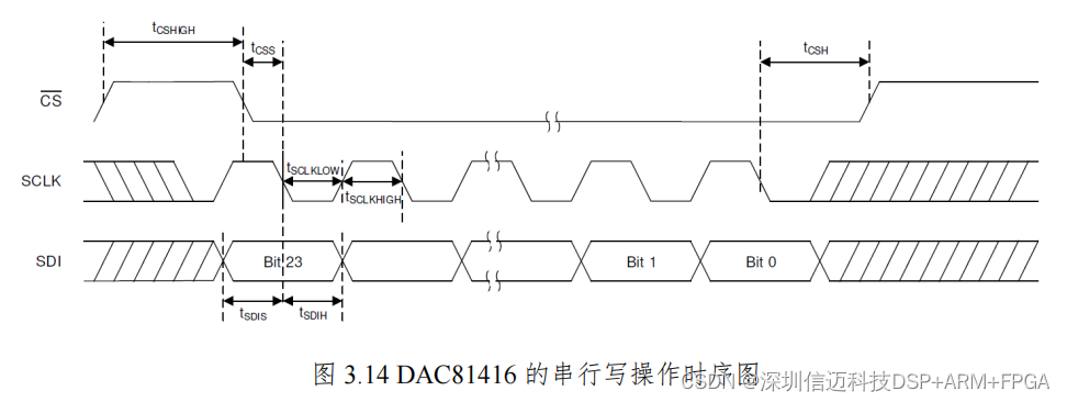
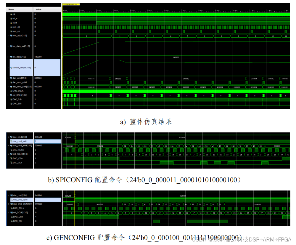
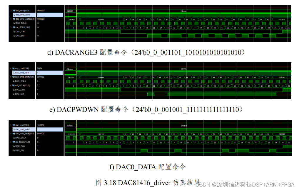
The DAC81416 (Texas Instruments) is a 16-channel, 16-bit digital-to-analog converter configured over an SPI serial interface supporting up to 50 MHz clock. Only SPI write operations are used in this design — no readback is required during normal operation.
The SPI write timing (Figure 3.14) follows a standard 24-bit frame: 8 address bits followed by 16 data bits, latched on the falling edge of SCLK at the DAC. This has a direct implication for the FPGA transmitter: because the DAC samples SDI on SCLK's falling edge, the FPGA must present stable SDI data aligned to SCLK's rising edge, providing maximum setup and hold margin.
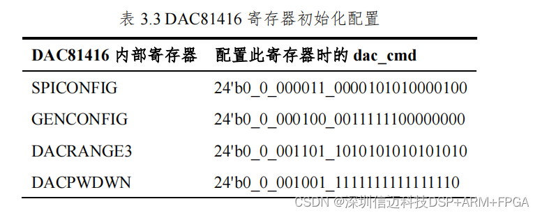
Before the DAC can produce accurate output voltages, it requires a power-on initialization sequence that configures internal registers (Table 3.3) — for example, output range selection, power-down mode settings, and LDAC (load DAC) behavior. Until initialization completes, the output voltages are indeterminate.
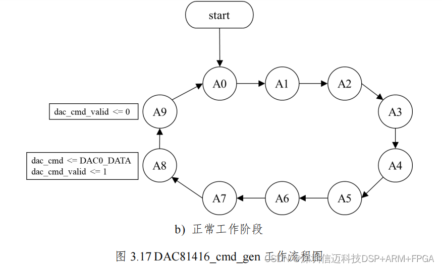
The DAC81416_driver module is composed of two sub-modules:
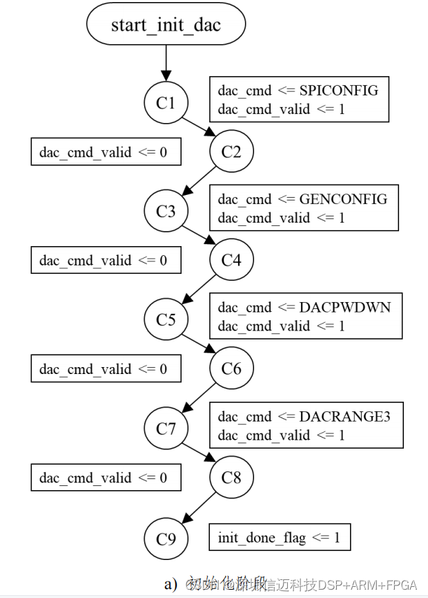
DAC81416_cmd_gen — generates the register-write command stream. It operates in two phases:
- Initialization phase: triggered by the
start_init_dacsignal from the PS. Writes each register in Table 3.3 in sequence and assertsinit_done_flagon completion. - Normal operation phase: begins only after
init_done_flagis set and the PS assertsstart. This two-gate condition prevents the DAC from outputting voltages before both hardware initialization and software authorization are confirmed.
During normal operation the module is slaved to the main control state machine, which has a 1 ms period divided into 10 states of 0.1 ms each. DAC updates are issued only during states A8 and A9, concentrating the SPI traffic into a well-defined window within each control cycle.
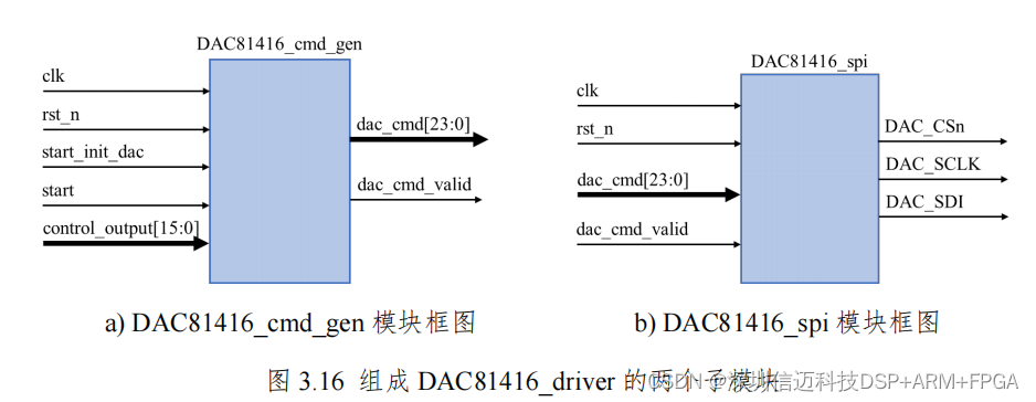
DAC81416_spi — serializes the parallel dac_cmd word from cmd_gen into the SPI bit stream. The key implementation detail here mirrors the timing constraint noted above: SDI transitions are aligned to SCLK rising edges so the DAC's falling-edge sampler always sees stable data.
Simulation results for the complete DAC81416_driver, including both the initialization handshake and the steady-state SPI write cycles, are shown below.
Sienovo provides a complete Zynq + AD7606 solution for industrial vibration control applications, covering hardware platform design, PL driver development, and PS software integration.