Custom Virtex-4 CameraLink Development Board with PCI Image Acquisition Card, FPGA-HDMI Encoding, and LVDS Camera Support
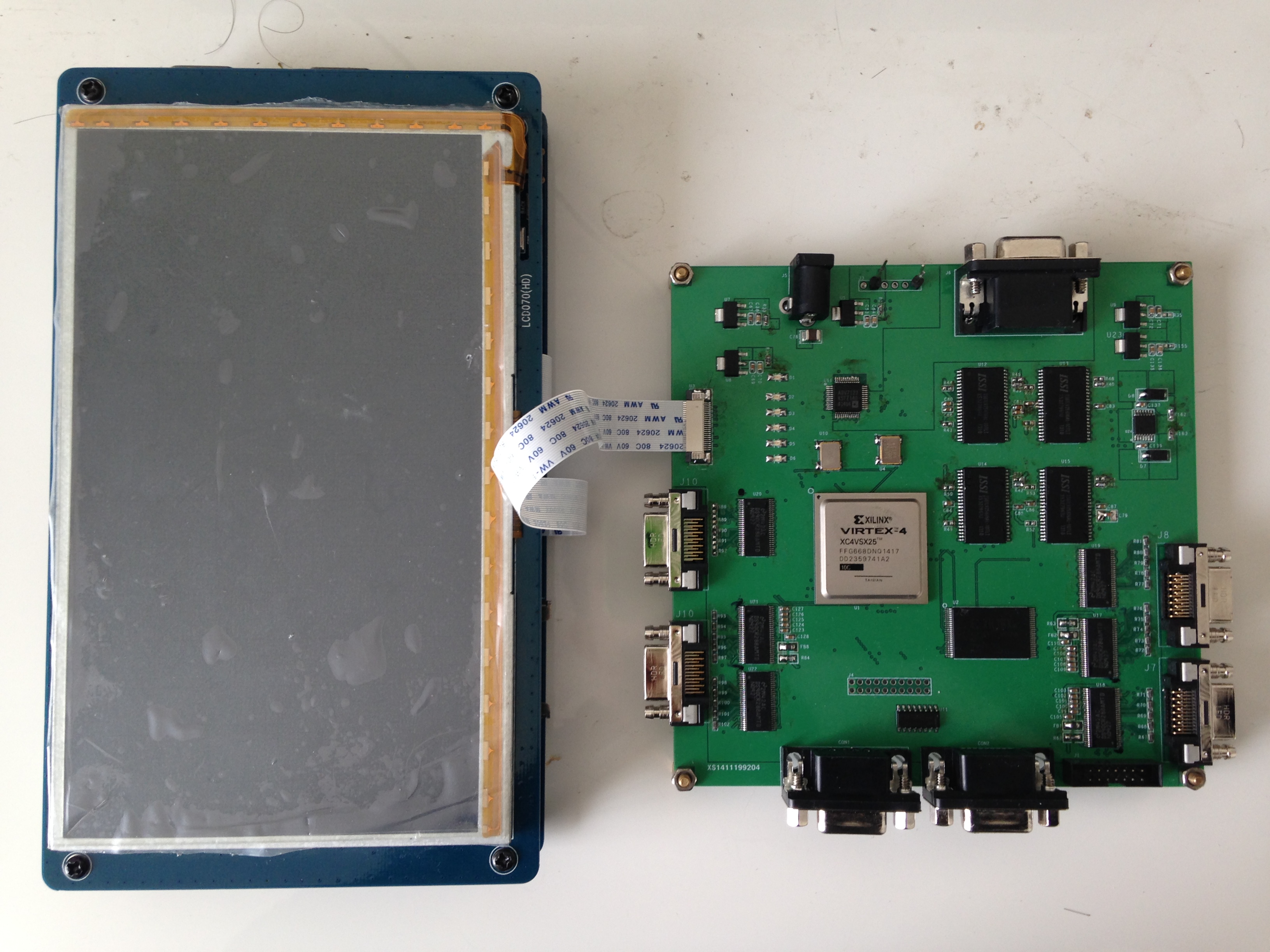
This custom Virtex-4 CameraLink development board is designed for industrial machine-vision and image-acquisition applications where high-speed camera data must be captured, buffered, and forwarded to a host processor — ARM or DSP — for real-time analysis. The board bridges the CameraLink physical layer to a standard FPC ribbon cable, making it straightforward to drop into existing embedded-vision pipelines without redesigning the camera front-end.
FPGA: Xilinx Virtex-4
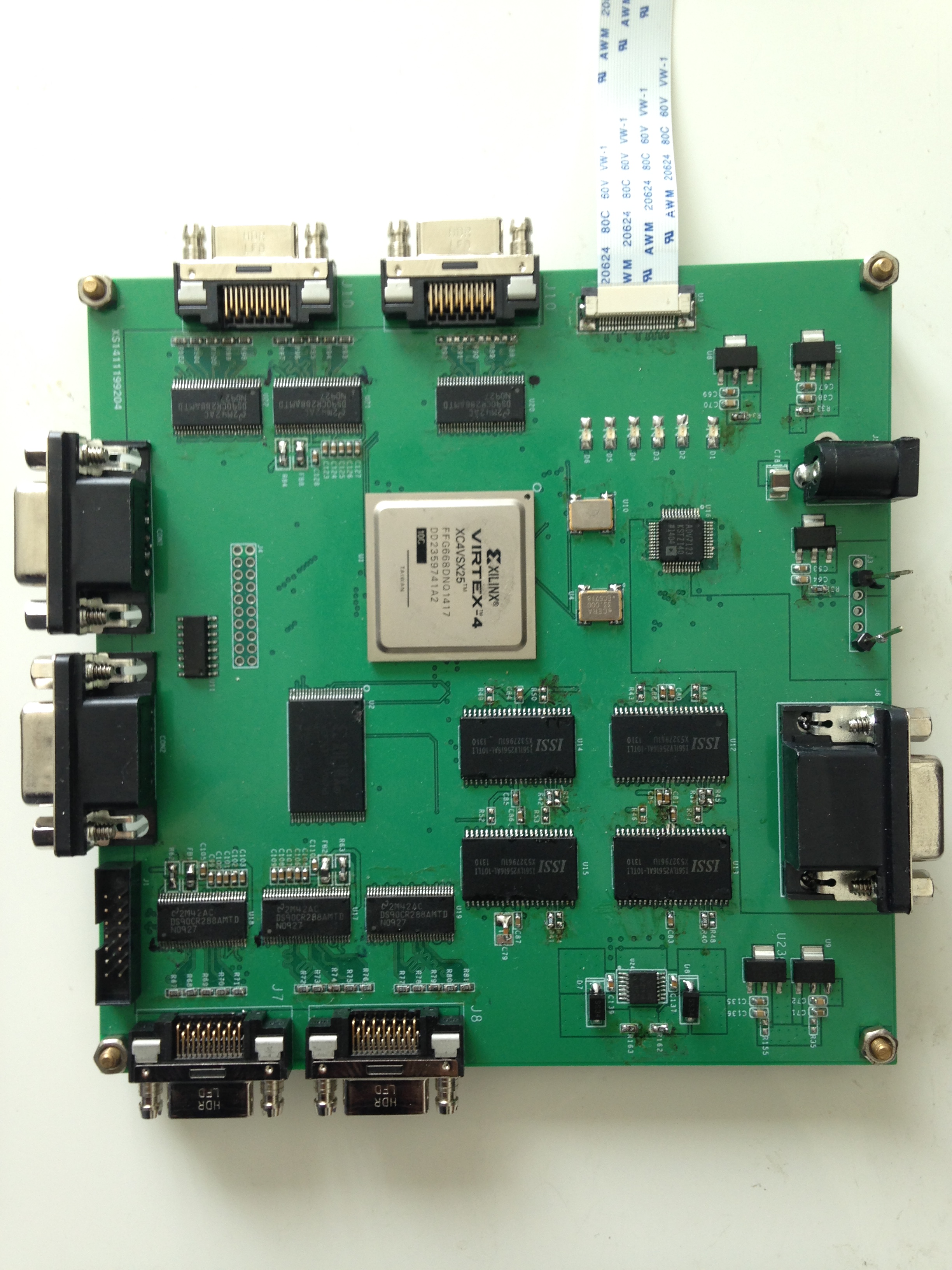
The board's logic fabric is built around a Xilinx Virtex-4 device. Virtex-4 parts include dedicated RocketIO serial transceivers and large block-RAM resources that suit them well for data-path applications: deserializing the high-speed LVDS streams from a CameraLink camera, packing pixels into frames, and writing burst transfers to the onboard SRAM. The Virtex-4 family also offers dedicated DSP48 slices, which can be used for in-FPGA preprocessing (histogram, colour conversion, simple filtering) before the data leaves the board.
CameraLink Interface: DS90CR288AMTD (Dual-Channel)
The physical CameraLink link is terminated by a pair of National Semiconductor (now Texas Instruments) DS90CR288AMTD deserializers. Each DS90CR288A converts a 28-bit LVDS serial stream back into 28 parallel LVCMOS/LVTTL data bits at the pixel clock rate. Running two of these ICs in parallel is exactly what is required for Full mode CameraLink, which uses a 4-tap configuration across two cable connectors. In Base mode a single 2-tap, 24-bit-wide configuration suffices, so only one of the two deserializer paths is active.
Base Mode vs. Full Mode
| Parameter | Base | Full |
|---|---|---|
| Cable connectors | 1 | 2 |
| Data taps | 2 | 4 |
| Max pixel bandwidth | ~255 MB/s | ~680 MB/s |
| Typical use case | Standard cameras, line-scan at moderate rates | High-speed area-scan, multi-tap line-scan |
Supporting both modes on a single board means the same hardware can be reused across camera generations without a PCB respin — a common requirement in industrial automation where cameras are upgraded independently of the processing pipeline.
Onboard RAM: IS61LV25616AL ×4
Four ISSI IS61LV25616AL static RAM devices are fitted onboard, each providing 256 K × 16-bit storage. Populated in parallel, the combined capacity is 1 M × 16 bits (2 MB) with an aggregate 64-bit-wide bus to the FPGA. SRAM is favoured here over SDRAM for its zero-latency random-access behaviour: the FPGA can write pixels as they arrive from the deserializer, then read them back in a different order (line-buffering, frame-synchronisation) without the refresh and burst-alignment overhead of a DRAM controller. The 8 ns (−8 suffix) or 10 ns speed grade typical for this part comfortably meets the pixel-clock requirements of even Full-mode CameraLink streams.
Onboard VGA Output: ADV7123
The Analog Devices ADV7123 is a triple 10-bit, 330 MSPS video DAC capable of driving a standard 75 Ω VGA load directly. Its presence on the board enables local monitoring: the FPGA can route a live pixel stream or a debug overlay out to any VGA monitor without involving the host ARM/DSP. This is particularly useful during bring-up and calibration — the operator can visually confirm camera exposure, focus, and synchronisation signals before enabling the downstream data path.
Host Interface: FPC Ribbon Cable to ARM / DSP
Rather than a PCI or PCIe edge connector, this board uses an FPC (Flexible Printed Circuit) ribbon cable to connect to the host processor board. The FPC interface carries pixel data, control signals, and the two serial (UART) ports to standard ARM and DSP development boards commonly found in the embedded-vision ecosystem (e.g., TI OMAP, AM335x, or AM572x carrier boards). This keeps the integration cost low: no custom PCIe driver is required, and the same ribbon cable connector footprint is widely available on evaluation hardware.
Peripheral Interfaces
- Two serial ports (UART): Used for camera configuration (most CameraLink cameras expose a GenICam or proprietary serial command channel over the CameraLink cable's serial pins, which the FPGA extracts and routes to a UART) and for board-level debug logging.
- GPIO: General-purpose I/O for trigger signals, strobe outputs, or external synchronisation with lighting controllers — a standard requirement in factory-floor vision systems.
Typical Integration Flow
- Camera connection: Attach a CameraLink camera to the MDR-26 connector(s). Choose Base (one cable) or Full (two cables) depending on the camera's output mode.
- FPGA configuration: Load the Virtex-4 bitstream via JTAG. The FPGA initialises the DS90CR288AMTD deserializers and begins accepting pixel data.
- Frame buffering: Incoming pixels are written to the IS61LV25616AL SRAM frame buffer. The FPGA handles sync signal separation (FVAL, LVAL, DVAL) to delineate frames and lines.
- Host readout: The ARM or DSP host reads pixel data from the FPGA through the FPC ribbon cable interface, typically via a parallel bus or a high-speed GPIO protocol implemented in the FPGA.
- Local monitoring: The ADV7123 DAC outputs a VGA signal simultaneously, giving an operator live visual feedback without consuming host CPU cycles.
The board's combination of a high-capacity FPGA, dual CameraLink deserializers, low-latency SRAM, and flexible host interface makes it a solid starting point for industrial image-acquisition projects that need to support multiple camera configurations without committing to a specific host platform from the outset.