Collection of DSP+ARM (OMAPL138) Industrial Applications, and How DSP and FPGA Collaborate
First, why is DSP needed? Instead of popular FPGA SoCs like ZYNQ 7000? Is it power consumption? Cost? Or specific application scenarios?
I. Industrial Image Acquisition and Recognition
- Design and Implementation of a Digital Display Instrument Character Recognition System Based on OMAPL138: Character Image Recognition
- Design and Implementation of an Elderly Care System Based on Video Image Analysis
II. Communication
- Development of an Underwater Acoustic Communication Signal Processing System
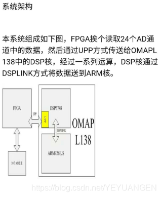
This article primarily focuses on driver development for the communication interface between the OMAP core board and FPGA, including GPIO control drivers and UPP data bus drivers for the interface. The character device drivers are designed using methods such as ioctl and memory mapping. For the OMAPL138 dual-core processor, DSPLINK is used for dual-core communication development in this paper, enabling data exchange and collaborative operation between the underwater acoustic communication software running on the DSP core and the embedded Linux system running on the ARM core.
The digital signal processing platform is a crucial component of an underwater acoustic modem, responsible for implementing modulation and demodulation algorithms in underwater acoustic communication. Considering the characteristics of underwater acoustic communication, the digital signal processing platform must meet the requirements for high-speed data processing, be highly integrated in terms of hardware, and ensure low power consumption.
Therefore, OFDM technology is highly practical for underwater acoustic communication systems. Timing synchronization is a key aspect of OFDM technology; this paper implements timing synchronization using matched filters, with the specific algorithm employing the overlap-save method for signal correlation. However, systems applying OFDM technology still require extensive and complex digital signal processing, necessitating powerful digital processing components. The OMAP L137 chip features both an ARM core and a DSP core, capable of handling both transaction-intensive and computation-intensive tasks, and includes audio acceleration hardware, making it highly suitable as a hardware platform for underwater acoustic communication systems.
MPSK-FMT modulation was completed, UPP communication between OMAPL138 and FPGA was established, and signal post-processing such as Hilbert transform, matched filtering, carrier symbol timing synchronization, and adaptive equalization were implemented on the OMAPL138.
- Design of a Multi-Core Attitude Measurement System
This solution uses a dual-core architecture with ARM as the communication and control processor and DSP as the integrated navigation solution processor as the main core, with FPGA serving as an auxiliary core for collecting MEMS gyroscope data and GPS module data.
- Design of a Wireless Sensor Network Node Based on OMAPL138 Chip
III. Industrial Control
- Application and Development of FPGA in Embedded Spray Painting Robot Controllers
In the controller, the ARM core of OMAPL138 is responsible for communication with the robot's operating interface and system management; the DSP core handles robot coordinate transformation, joint interpolation, sampled information processing, and assistance algorithms; and the FPGA is responsible for controlling and detecting robot equipment.
For servo signal sampling, position/torque control and switching, as well as I/O device signal detection and control, the software design and implementation of an FPGA-based spray painting robot controller were studied, including incremental pulse sampling modules, DAC controllers, digital/pulse conversion modules, and I/O monitoring modules, providing underlying support for achieving spray painting robot teaching, assistance, and reproduction.
- Motion Controller
High-Speed Interface Design for Heterogeneous Multi-Core Motion Controllers
ARM9 embeds a Linux operating system to enhance the controller's multi-task coordination capabilities; the DSP does not run an operating system, ensuring real-time computation. The focus is on the high-speed interface design and firmware design for communication between ARM and DSP, DSP and FPGA, and the controller and PC. Experiments show that this motion controller has high data exchange rates, large throughput, and high stability, providing a reference for high-speed communication interfaces in heterogeneous multi-core controllers.
- High-Speed Signal Acquisition and Processing
IV. Power
- Design of Power Data Acquisition and Transmission Based on OMAPL138
This solution uses Texas Instruments' OMAPL138 microprocessor as its core, utilizing the microprocessor to analyze and process collected data such as voltage, current, and switch inputs, and transmits data to the host computer via interfaces like RS 485/RS 232 and Ethernet using various protocols.
- Design of a Power Quality Monitoring System Based on OMAPL138
1 Evaluation Board Introduction Based on TI OMAP-L138 (fixed/floating point DSP C674x+ARM9) + Xilinx Spartan-6 FPGA processor; OMAP-L138 and FPGA are connected via uPP, EMIFA, and I2C buses, with communication speeds up to 228 MByte/s; OMAP-L138 operates at 456MHz, offering computing power up to 3648 MIPS and 2746 MFLOPS; FPGA is compatible with Xilinx Spartan-6 XC6SLX9/16/25/45, providing strong platform upgrade capabilities; The development board exposes rich peripherals, including high-speed data transfer interfaces such as Gigabit Ethernet, SATA, EMIFA, uPP, USB 2.0, as well as common interfaces like GPIO, I2C, RS232, PWM, and McBSP; Certified through high and low-temperature tests, suitable for various harsh working environments; DSP+ARM+FPGA triple-core module, with dimensions of 66mm*38.6mm, uses industrial-grade B2B connectors to ensure signal integrity; Supports bare-metal, SYS/BIOS operating system, and Linux operating system.
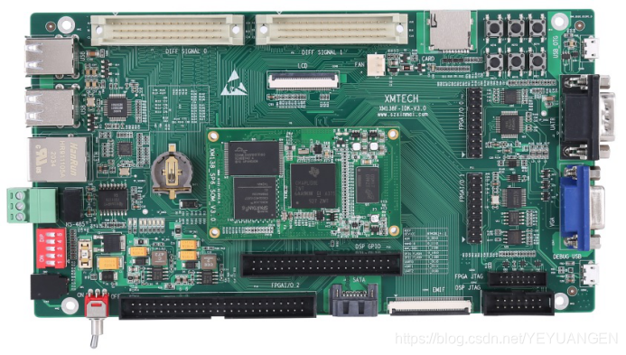 Figure 1 Front and Side Views of the Development Board
The XM138F-IDK-V3.0 is a development board designed based on the Sienovo XM138-SP6-SOM core board, featuring a 4-layer board design with immersion gold and lead-free processes. It provides users with a test platform for the XM138-SP6-SOM core board, enabling rapid evaluation of its overall performance.
The XM138-SP6-SOM exposes all CPU resource signal pins, making secondary development extremely easy. Customers only need to focus on upper-layer applications, significantly reducing development difficulty and time costs, allowing products to quickly enter the market and seize opportunities. It not only provides rich demo programs but also detailed development tutorials and comprehensive technical support to assist customers with baseboard design, debugging, and software development.
2 Typical Application Areas
Data Acquisition, Processing, and Display Systems
Smart Power Systems
Image Processing Equipment
High-Precision Instrumentation
Mid-to-High-End CNC Systems
Communication Equipment
Audio and Video Data Processing
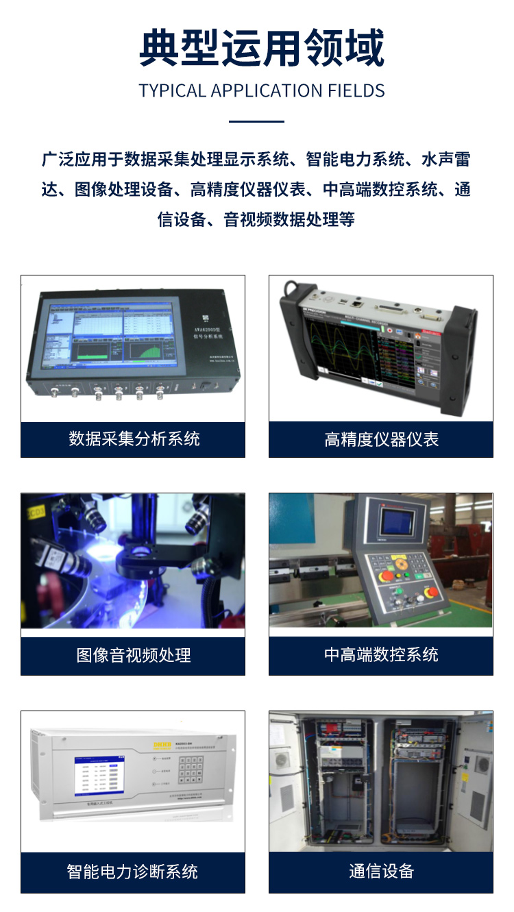
Figure 2 Typical Application Areas
3 Hardware and Software Parameters
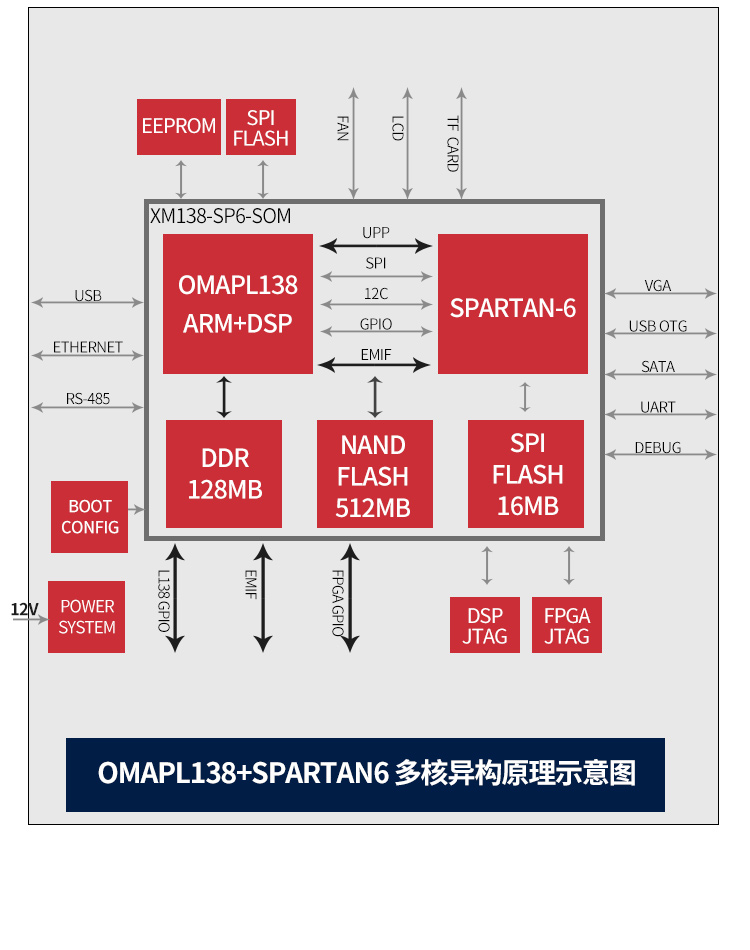 Schematic Diagram of Development Board Peripheral Resources
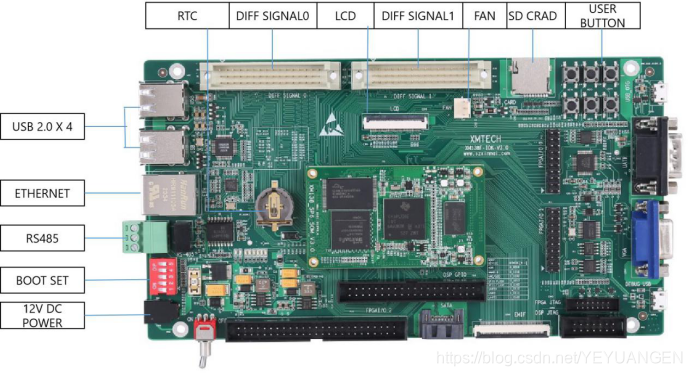
Figure 3 Schematic Diagram of Development Board Interfaces
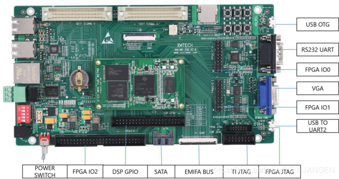
Figure 4 Schematic Diagram of Development Board Interfaces
