Differences in NOR Flash and NAND Flash Boot Processes on mini2440
Goal: Thoroughly read the mini2440 manual
I. Debugging Experience
-
A tip from an old computer scientist: When you encounter strange problems, restarting is one of the simplest solutions, because operating systems themselves have imperfections, whether it's Microsoft Windows or Apple computers.
-
USB-to-serial cable experiencing garbled characters: This indicates unstable functionality and performance of the serial cable. A high-performance one can be purchased to replace it.
II. Q&A
1. What are NAND and NOR? What are the differences and connections between NAND boot and NOR boot? (Compiled and organized)
Answer: 1) Code can be executed directly from NOR Flash, but not from NAND Flash. In the 2410, if NAND boot mode is selected, the code in NAND is copied to RAM for execution.
-
Before each data read, NAND Flash seems to require writing 0x55, 0xAA, while NOR Flash directly retrieves data.
-
NOR Flash has separate address and data lines; data is output when address and control signals are received. NAND Flash has shared address and data lines and requires programmatic control to output data.
2. How to boot into BIOS mode?
Answer: Simply set the S2 jumper switch to the NOR flash side.
3. SuperVivi is used as the bootloader, while some development boards use U-Boot.
4. What does SEC s3c241x mean?
III. Differences in ARM's NOR Flash and NAND Flash Boot Processes
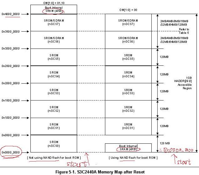
Detailed explanation of s3c2440 boot process 1: Address space allocation 2: Development boards generally use SDRAM as memory, and flash (NOR, NAND) as ROM. NAND flash has no address lines, and at least one page (512B) must be read at a time. The other two have address lines. 3: NAND flash is not used to run code, only to store code. NOR flash and SDRAM can execute code directly. 4: The s3c2440 has a total of 8 memory banks. 6 memory banks can be used as ROM or SRAM. The remaining 2 banks can be used as SDRAM in addition to ROM or SRAM (different memory types have different read/write methods). The starting addresses of 7 banks are fixed. There is also one flexible bank whose memory address and size can be changed. 5: The s3c2440 supports two boot modes: NAND and non-NAND (which refers to NOR flash here). The specific method adopted depends on the OM0 and OM1 pins. Boot mode determined by OM[1:0]: When OM[1:0]=00, the processor boots from NAND Flash. When OM[1:0]=01, the processor boots from 16-bit wide ROM. When OM[1:0]=10, the processor boots from 32-bit wide ROM. When OM[1:0]=11, the processor boots from Test Mode.
- At the factory, the development board has the same BIOS burned into both NAND flash and NOR flash.
When booting from NAND,
the CPU automatically reads the first 4KB of data from NAND flash and places it into the on-chip SRAM (the s3c2440 is an SoC), and simultaneously maps this on-chip SRAM to the nGCS0 chip select space (i.e., 0x00000000). The CPU starts execution from 0x00000000, which is the first 4KB of content from NAND flash. Because NAND Flash does not even have address lines, it cannot directly map NAND to 0x00000000, so it must use the on-chip SRAM as a carrier. Through this carrier, larger code from NAND flash is copied to RAM (usually SDRAM) for execution.
When booting from non-NAND flash,
NOR flash is mapped to address 0x00000000 (which is nGCS0; here, on-chip SRAM is not needed for assistance, so the starting address of the on-chip SRAM is still 0x40000000). Then the CPU starts execution from 0x00000000 (i.e., executes in NOR flash).