A Comprehensive Analysis of the AMD XCVU13P (VU13P)-based 400G FPGA AI Network/Scientific Accelerator Card XM-APU4090, for NVIDIA GPU Replacement, High-Performance Computing, and More
A Comprehensive Analysis of the AMD XCVU13P (VU13P)-based 400G FPGA Network/ Scientific Accelerator Card XM-APU4090
Chip and Processor
I. Introduction: The 400G Era, Performance Bottlenecks of Traditional CPUs and Standard NICs
As data centers, High-Performance Computing (HPC), low-latency trading, and distributed storage services fully enter the 400G era, traditional 10GbE/100G standard NICs and pure CPU software protocol stack architectures reveal unavoidable shortcomings:
-
Processing massive packets, TCP/IP tunnel encapsulation, RDMA, and NVMe-oF protocols all rely on the CPU, consuming significant core compute power and incurring a high "compute tax." Actual tests in virtualized environments show CPU utilization can exceed 30%.
-
Frequent memory copies between kernel and user space, along with interrupt context switching, introduce tens of microseconds of jitter, failing to meet the deterministic low-latency requirements of quantitative trading and HPC simulations.
-
The CPU's serial computing architecture struggles to process 400G line-rate packets in parallel, leading to throughput collapse and spiking tail latency under high concurrency.
Programmable SmartNICs/DPUs have emerged as the optimal solution. AMD Virtex UltraScale+ XCVU13P (VU13P), as a flagship 16nm FPGA, boasts millions of logic cells, tens of thousands of DSPs, and hundreds of Gbps GTY high-speed SERDES, making it the ideal chip for building 400G high-performance acceleration hardware. This article will provide an in-depth breakdown of the VU13P-based XM-APU4090 dual-purpose accelerator card, which addresses two core scenarios: intelligent network offload and scientific parallel computing acceleration.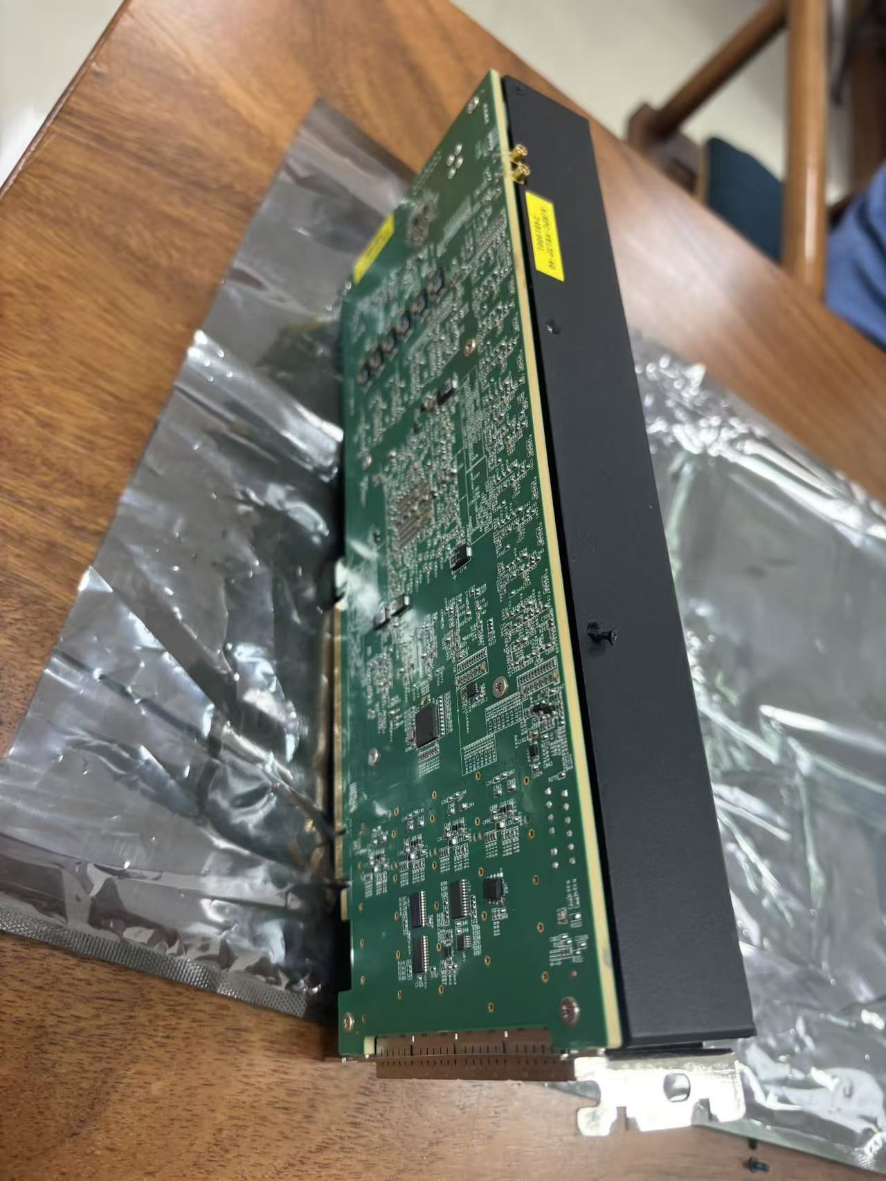
II. Core Hardware Foundation: AMD XCVU13P Chip Capabilities
The XM-APU4090 uses the XCVU13P as its processing core. Let's first outline the chip's underlying hardware resources to understand the accelerator card's performance ceiling:
Operating System
-
Logic and Compute Resources
-
3780K system logic cells, 12288 DSP48E slices, with INT8 compute power up to 38 TOPS, suitable for scientific simulation, signal processing, and AI inference parallel computing.
-
Total on-chip memory of 455Mb (Block RAM + UltraRAM), a large on-chip cache that reduces DDR access latency, supporting line-rate packet caching and large-scale matrix operations.
-
-
High-Speed Serial Transceiver GTY Integrated 128 GTY SERDES lanes, with a single-lane rate of 32.75Gbps, natively supporting QSFP28 100G optical ports. The XM-APU4090 reuses 4 sets of GTY lanes to achieve 4×100G Ethernet, providing a total machine throughput of 400Gbps.
-
Hardened High-Speed Interface IP Integrates a native PCIe Gen3 x16 hard IP controller, which does not consume general-purpose logic, ensuring stable high-speed data communication between the host CPU and the FPGA.
-
Multi-SLR Partitioned Architecture 3-SLR multi-die stacking with ultra-high bandwidth interconnect between dies, solving the timing convergence challenges of deploying ultra-large algorithms, a complete 4-layer protocol stack, and storage controllers simultaneously.
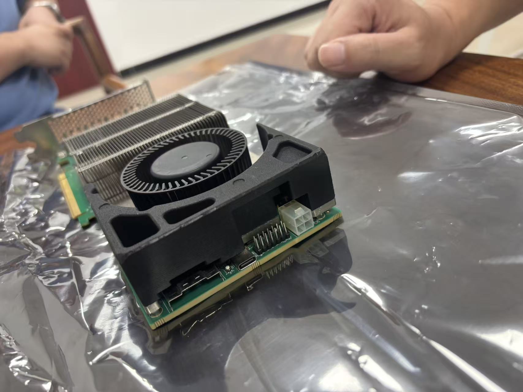
III. Detailed Specifications of the XM-APU4090 Accelerator Card
3.1 Hardware Parameter Summary
Parameter
XM-APU4090 Detailed Configuration
Core FPGA
AMD Virtex UltraScale+ XCVU13P
Host Interface
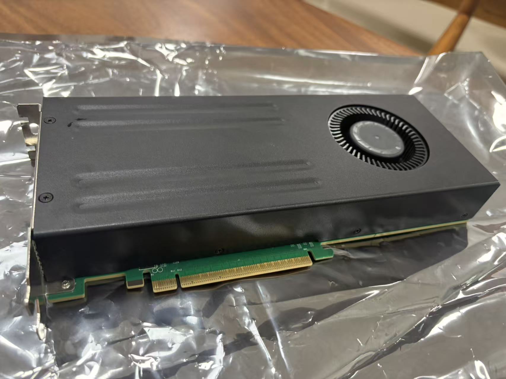
PCIe Gen3 x16, Dual-slot, Full-height, 3/4 length (111.1mm×254mm)
Network Interface
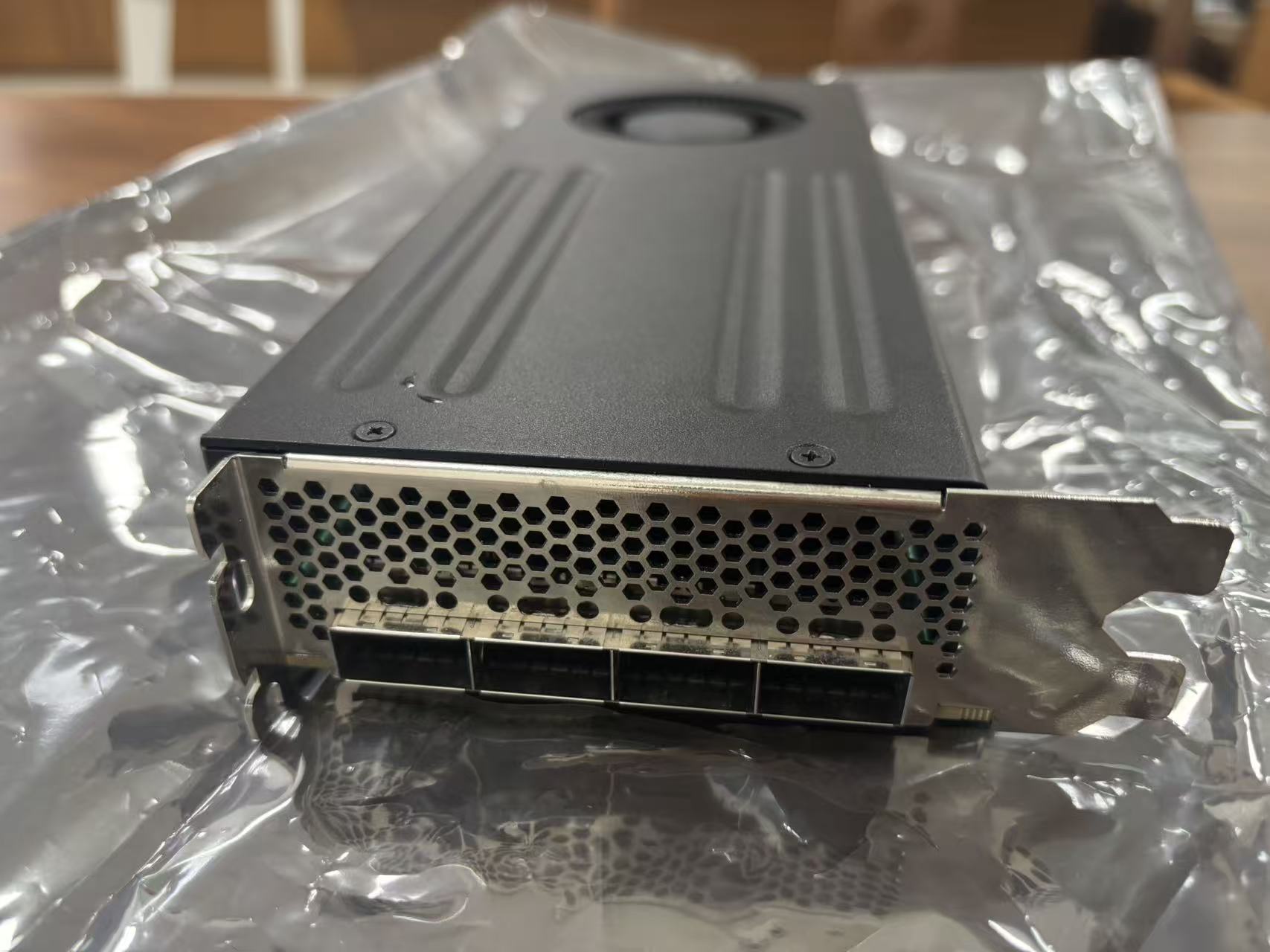
4×QSFP28, 100G per port, 400Gbps line-rate throughput for the entire card
Onboard Memory
32GB ECC DDR4-2666MT/s, hardware error correction ensures data reliability
Configuration Storage
2Gb QSPI Flash, supports dual-image firmware online upgrade
Storage Expansion
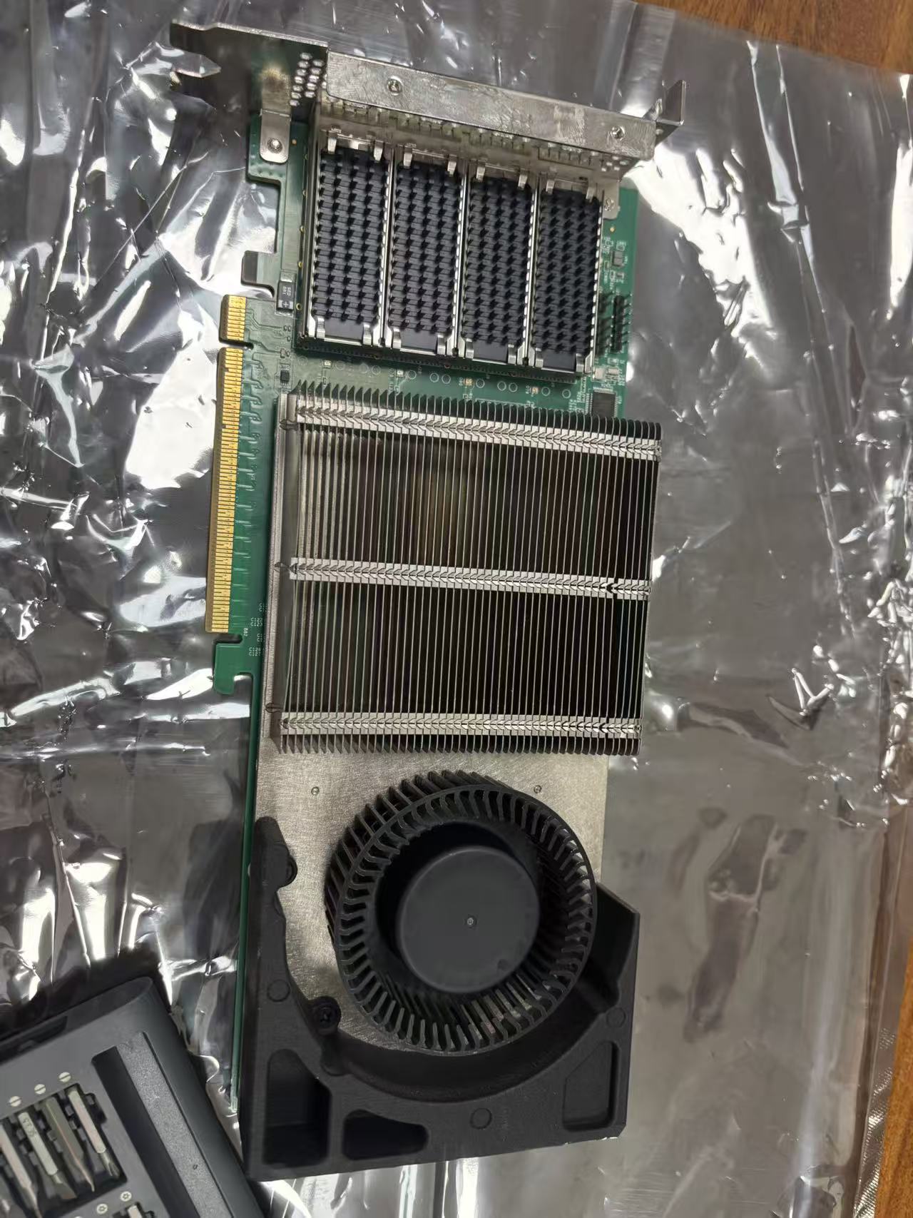
SlimSAS interface, supports mounting 2 PCIe Gen3 U.2 NVMe SSDs, native NVMe-oF acceleration
Clock Synchronization
2 SMA external clock interfaces: 1 PPS (Pulse Per Second) input, 1 10MHz reference clock input, meeting high-precision synchronization for PTP / Time-Sensitive Networking (TSN)
Cooling
Standard server active cooling, suitable for 24/7 continuous operation in data centers
Form Factor
Standard PCIe add-in card, compatible with x86 servers, HPC compute nodes
3.2 Three Innovative Designs in Hardware Architecture
1. Dual Acceleration Paths for Network + Storage, One Hardware Platform Covering Two Major Applications
Traditional accelerator cards either focus solely on network offload or only on compute acceleration. The XM-APU4090 achieves parallel dual data streams through hardware partitioning:
-
Network Path: GTY → FPGA packet processing logic → PCIe direct to host, hardware offloading TCP/UDP, VxLAN, OVS, RDMA.
-
Storage Path: SlimSAS NVMe direct to FPGA, hardware implementation of NVMe-oF remote storage protocol, without CPU intervention.
-
Scientific Computing Path: Host dispatches matrix/simulation data via PCIe to the 32GB large DDR, FPGA DSP array performs parallel computation, and results are returned to the CPU.
2. Large ECC Memory, Suitable for Large-Scale HPC Scientific Simulations
The onboard 32GB ECC DDR4 is a high-end configuration among VU13P NICs of similar specifications:
-
Scientific Computing Scenario: Caches massive intermediate simulation data and multi-dimensional matrices, avoiding frequent host memory access that leads to PCIe bandwidth contention.
-
Network Scenario: Caches millions of concurrent packet queues at 400G line rate, eliminating congestion and packet loss, and supporting zero-copy data transfer.
3. Industrial-Grade High-Precision Clock Synchronization
Dual SMA clock interfaces are a critical requirement for finance, industrial, and distributed HPC clusters:
-
PPS + 10MHz external reference, enabling sub-microsecond cluster time synchronization.
-
Suitable for quantitative trading, distributed simulation, 5G transport, and industrial TSN low-latency scheduling scenarios.
IV. Two Core Orientations: Intelligent Network Acceleration + High-Performance Scientific Computing Acceleration
4.1 Orientation One: 400G FPGA SmartNIC (Data Center Network Offload)
Core Hardware Offload Capabilities (Helicon-213-B Acceleration Engine)
All network tasks traditionally handled by the CPU are offloaded to FPGA hardware, achieving three major benefits: CPU offloading, low latency, and low power consumption:
-
Full Protocol Stack Hardware Offload TCP/IP fragmentation and reassembly, VLAN/VxLAN tunnel encapsulation and decapsulation, IPsec/TLS encryption and decryption, and RDMA RoCEv2 are all implemented in hardware. The host CPU only handles application logic, reducing network processing CPU utilization by over 90%.
-
Virtualization Acceleration Hardware SR-IOV and OVS flow table offload improve virtual machine network forwarding performance in cloud data centers by 5 times, eliminating virtualization compute overhead.
-
400G Line-Rate Non-Blocking Forwarding All 4×100G QSFP28 ports simultaneously achieve 400G throughput, with nanosecond-level packet pipeline processing and no software interrupt jitter.
-
NVMe-oF Storage Offload SlimSAS directly connects to two U.2 SSDs, with an integrated NVMe controller in the FPGA. Remote storage I/O completely bypasses the host kernel, significantly increasing distributed storage IOPS.
Typical Network Acceleration Application Scenarios
-
Low-Latency Trading Systems: Sub-microsecond end-to-end latency, no operating system kernel jitter, meeting the demands of high-frequency trading for securities and futures.
-
Large Cloud Data Centers: Cloud computing and virtualization clusters, freeing up server CPU compute power for applications.
-
Distributed Storage Clusters: 400G high-speed interconnect + hardware NVMe-oF, building low-latency distributed block storage.
-
5G Transport / Edge Gateways: Large-traffic edge data offloading, hardware traffic scrubbing, and packet filtering.
4.2 Orientation Two: VU13P High-Performance Scientific Computing Accelerator Card
Leveraging the XCVU13P's massive DSPs and large on-chip memory, it replaces CPUs/GPUs for parallel scientific simulation computations, offering advantages in deterministic latency, low power consumption, and customizable algorithms:
-
Applicable Scientific Computing Applications
-
Computational Fluid Dynamics (CFD), electromagnetic simulation, Finite Element Analysis (FEA).
-
Radar/satellite signal processing, broadband digital filtering, large-scale parallel FFT computations.
-
Small to medium-scale AI inference, real-time image parallel processing.
-
HPC cluster node coprocessing, offloading CPU matrix computation pressure.
-
-
Core Advantages for Scientific Computing
-
Programmable Pipeline Architecture: Customized hardware logic for simulation algorithms, with significantly lower power consumption than GPUs for equivalent compute power.
-
32GB ECC Large Cache: Supports local caching of ultra-high-dimensional matrices, reducing PCIe data interaction bottlenecks.
-
Synergy with Network Path: Simulation results can be directly dispatched to other cluster nodes via the 400G optical ports, providing integrated computation + transmission acceleration.
-
V. XM-APU4090 Core Advantages Compared to Similar Accelerator Cards
-
Dual-Purpose Integrated Hardware: The same card can function as both a 400G SmartNIC and a scientific computing accelerator, reducing data center hardware procurement costs and PCIe slot usage.
-
Flagship VU13P Compute Power Foundation: Compared to VU9P and VU7P accelerator cards, logic, DSP, and GTY resources are doubled, supporting more complex protocols and large-scale simulations.
-
32GB ECC Large Capacity Memory: Most VU13P NICs on the market only have 8GB/16GB DDR. This card's large cache adapts to 400G high concurrency and large-scale scientific simulations.
-
Native NVMe Expansion + High-Precision Clock: Standard SlimSAS and dual SMA clock interfaces are ready-to-use for finance, HPC, and storage scenarios.
-
Flexible Customization + Comprehensive Technical Services: Standard products delivered from stock, supporting customer customization of FPGA firmware logic. Provides 24-hour technical support, a one-year hardware warranty, and complete Linux/DPDK/RDMA drivers.
VI. Development and Deployment Notes
-
Software Ecosystem Support
-
Operating Systems: CentOS, Ubuntu mainstream Linux distributions.
-
Data Plane: DPDK user-space drivers, RDMA RoCE drivers, SR-IOV virtualization drivers.
-
Development Tools: AMD Vitis, Vivado, with open board hardware constraint files, allowing customers to independently develop network offload IPs and scientific computing algorithms.
-
-
Deployment Environment Standard 2U/4U x86 servers, with an available dual-slot PCIe Gen3 slot. A standard data center air-cooled environment is sufficient for stable 24/7 operation.
-
Secondary Development Directions
-
Network-side: Custom packet filtering, traffic scheduling, encryption algorithms, proprietary tunnel protocols.
-
Compute-side: Hardware development of FFT, matrix multiplication, filtering, AI operators, and simulation pipelines.
-
VII. Conclusion
The XM-APU4090, as a dual-scenario flagship acceleration hardware based on AMD XCVU13P, bridges two major technical domains: 400G high-speed network offload and high-performance scientific parallel computing. In scenarios such as data center cost reduction and efficiency improvement, HPC simulation compute power enhancement, financial low-latency trading, and distributed storage, it perfectly addresses industry pain points like CPU compute bottlenecks, network latency jitter, and the high cost of multi-card hardware stacking.
For FPGA development engineers, data center architects, and HPC researchers, this card is both a commercially available 400G SmartNIC and a fully resourced VU13P algorithm validation hardware. It caters to both mass production deployment and algorithm R&D needs, making it the preferred platform for heterogeneous acceleration in the 400G bandwidth era.