Domestic RK3576+FPGA Architecture | Integrated Solution for Wafer Transfer Robot High-Speed Positioning + AI Defect Detection
Domestic RK3576+FPGA Architecture | Integrated Solution for Wafer Transfer Robot High-Speed Positioning + AI Defect Detection
I. Industry Pain Points and Solution Introduction
In semiconductor wafer manufacturing processes, wafer transfer robots undertake the core tasks of wafer loading/unloading, process flow, and precision alignment and transfer. They are critical connecting equipment for etching, thin film deposition, inspection, and packaging processes. Such equipment places stringent dual requirements on control systems: first, micron-level high-speed precision motion positioning, smooth start/stop without jitter, and high timing stability to prevent wafer collision, displacement, or breakage; second, real-time online appearance inspection capability to quickly identify defects such as wafer chipping, scratches, stains, and missing corners, ensuring factory yield.
Current mainstream industry solutions commonly adopt a split architecture of "imported motion controller + independent vision industrial PC," which presents numerous pain points: low equipment integration, bulky size, high data interaction latency between multiple devices, high software and hardware adaptation costs, and complex operation and maintenance. Meanwhile, traditional single ARM industrial control solutions lack sufficient real-time performance to meet high-speed motion synchronization requirements. Pure FPGA solutions lack a complete operating system ecosystem, making it difficult to implement intelligent functions such as AI inference, task scheduling, and data statistics, thus failing to meet the current intelligent upgrade demands of semiconductor equipment.
To address these industry pain points, this article introduces a domestic RK3576+FPGA heterogeneous integrated solution. It deeply integrates FPGA hard real-time motion control, high-speed machine vision acquisition, and RK3576 edge AI defect detection capabilities. A single device achieves integrated functions of high-speed wafer transfer positioning + real-time defect detection, significantly streamlining equipment structure, reducing mass production costs, and enhancing equipment automation and intelligence levels. It is perfectly suited for high-precision, high-reliability, and intelligent production scenarios in semiconductor cleanrooms.
II. Overall System Architecture Design
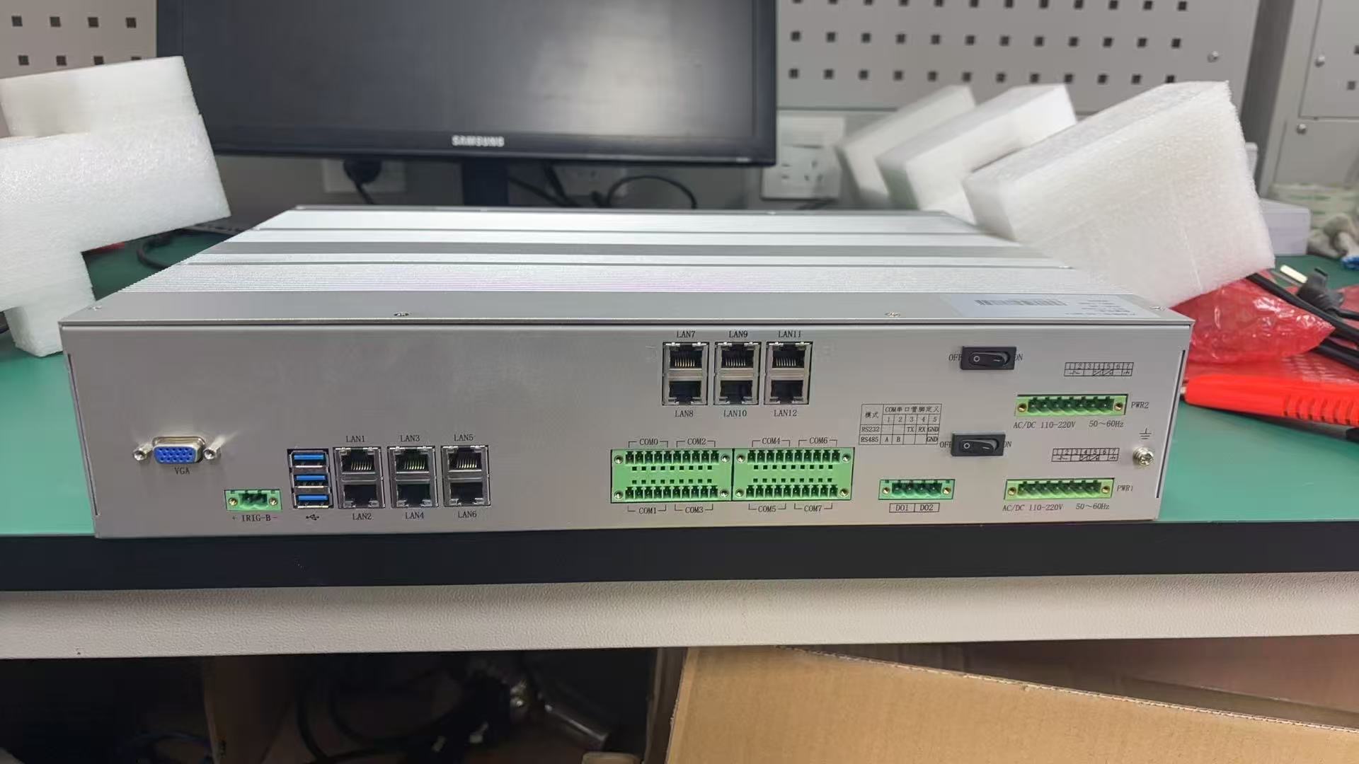
This solution adopts a RK3576 intelligent business AI layer + FPGA hard real-time control and pre-processing layer heterogeneous collaborative architecture. The software and hardware have clear divisions of labor and complementary advantages, retaining the flexible development ecosystem of embedded systems while possessing nanosecond-level real-time control capabilities of FPGA. This perfectly addresses the shortcomings of traditional split solutions, such as high latency, low integration, and lack of intelligent computing power.
2.1 RK3576 Core Capabilities (Decision Scheduling + Edge AI Computing Layer)
The RK3576 is a domestic high-performance industrial-grade master control chip, offering balanced computing power, low power consumption, wide temperature stability, and a complete ecosystem. It is fully adapted for industrial equipment operating 7x24 hours continuously. Its core functions are as follows:
- Equipped with a quad-core A76 + quad-core A53 heterogeneous architecture, providing sufficient computing power and controllable power consumption. It is responsible for overall machine task scheduling, wafer transfer path planning, process logic control, equipment status management, host computer communication, and data log storage.
- Built-in dedicated NPU computing power supports real-time edge inference for lightweight YOLO, image segmentation, and classification/detection models. It can independently complete the identification, classification, positioning, and statistics of various wafer appearance defects without an external industrial PC.
- Leveraging the complete Linux software ecosystem, it supports rapid secondary development, function iteration, and protocol adaptation. It can flexibly integrate with semiconductor production line MES systems and adapt to customized requirements of different process equipment.
- Rich network, serial, and peripheral interfaces support remote debugging, OTA upgrades, and data upload, meeting the needs of intelligent production line operation and maintenance.
2.2 FPGA Core Capabilities (Real-time Control + Image Pre-processing Layer)
As the underlying hard real-time core, the FPGA operates with full hardware logic, free from operating system scheduling latency. It focuses on solving low-latency, high-synchronization, and high-reliability issues for motion control and vision acquisition. Its core capabilities are as follows:
- Implements multi-axis linkage interpolation, high-speed position closed-loop control, and S-curve velocity smoothing algorithms for robots, with nanosecond-level response speed, completely eliminating high-speed motion jitter and lag issues, ensuring smooth wafer transfer.
- Directly interfaces with industrial high-frame-rate area scan cameras, performing high-speed image acquisition, hardware noise reduction, ROI cropping, and frame synchronization pre-processing. This significantly reduces image transmission data volume, lightens the RK3576's computing load, and achieves high-speed vision acquisition without frame loss.
- Hardware-level unified timing control binds motion trigger and camera capture signals, enabling simultaneous photo capture precisely at the moment the robot is in position. This solves missed detection and false detection issues caused by motion and vision desynchronization.
- Integrated hardware safety logic supports limit detection, emergency stop, abnormal self-locking, and power-off position memory, comprehensively ensuring the safe operation of wafer equipment and preventing material damage.
- Supports EtherCAT and CAN FD industrial bus expansion, adaptable for multi-axis servo linkage, meeting the control requirements of complex trajectory and multi-station wafer transfer equipment.
III. Core Key Technology Implementation
3.1 FPGA Hard Real-time Micron-level Motion Positioning Control
For multi-axis linkage scenarios of wafer transfer robots, including telescopic, rotary, and lifting axes, the FPGA independently performs hardware trajectory interpolation and closed-loop control, abandoning the latency defects of traditional software interpolation. Through real-time encoder position feedback, motion trajectories are dynamically corrected, combined with an S-curve velocity smoothing start/stop algorithm, effectively suppressing mechanical jitter and inertial deviation. This controls the overall machine positioning accuracy to ±0.005mm, fully meeting the precision transfer and alignment requirements for 8-inch and 12-inch semiconductor wafers, and adapting to high-frequency, continuous automated production modes on the production line.
3.2 Hardware Image Pre-processing + Edge AI Defect Detection
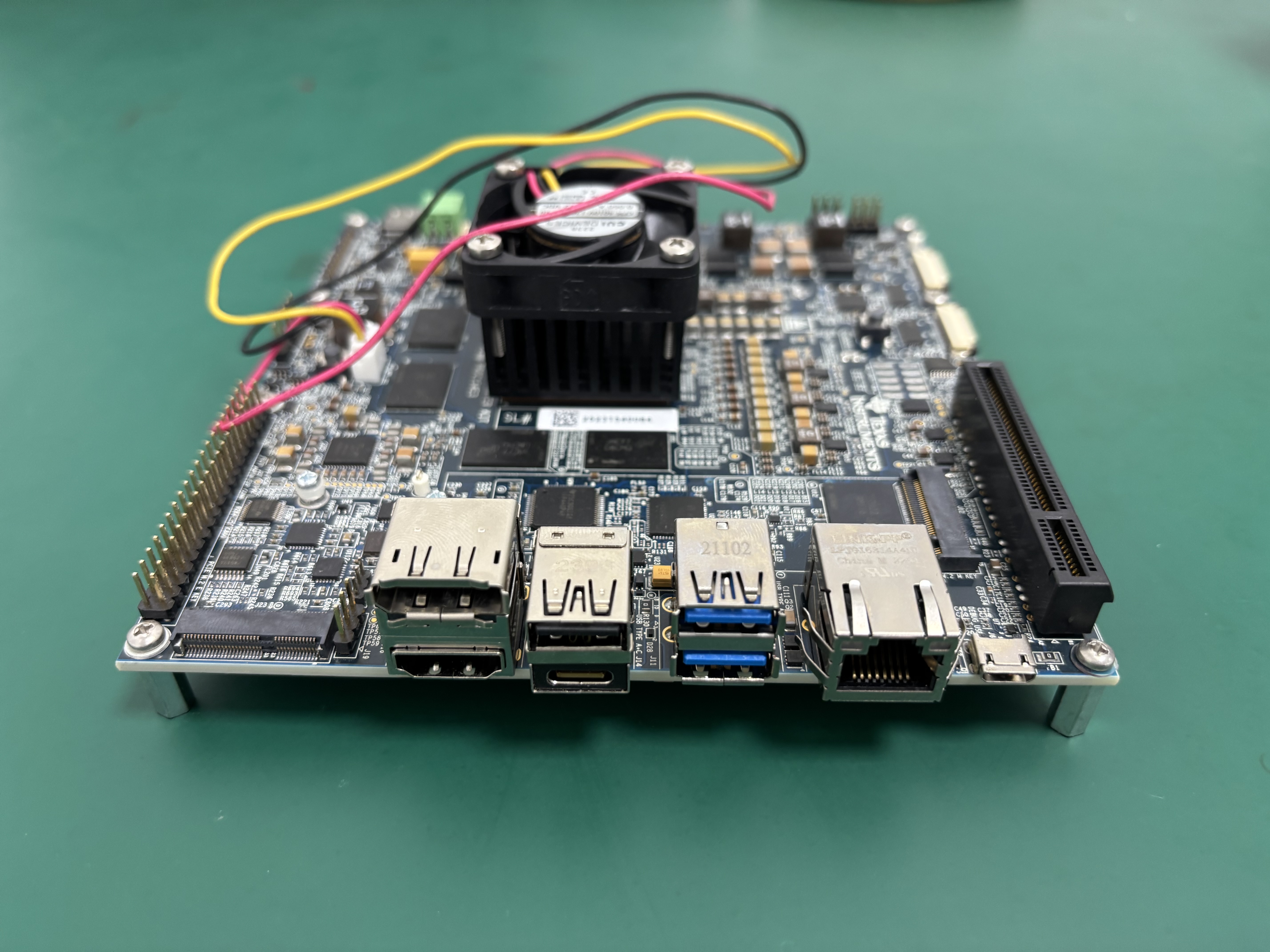
Traditional split vision inspection solutions suffer from image transmission delay, data packet loss, detection lag, and high equipment redundancy. This solution utilizes FPGA hardware to perform image pre-processing, automatically removing invalid backgrounds, performing image denoising, and precise cropping, transmitting only the effective wafer image regions to the RK3576. Leveraging the built-in NPU computing power, intelligent identification and classification of wafer scratches, chipping, stains, pinholes, missing corners, and other defects are completed in milliseconds. This achieves an integrated closed-loop operation for the entire process of motion transfer, image acquisition, AI detection, and result output, with detection efficiency and accuracy far exceeding traditional solutions.
3.3 Motion-Vision Hardware Timing Synchronization Technology
A core technical highlight of the solution is hardware-level microsecond-level timing synchronization. The FPGA uniformly manages the robot's motion-in-position signal and the industrial camera's capture trigger signal, achieving seamless connection between motion stop and image acquisition. This completely eliminates detection errors caused by software and hardware timing deviations. It effectively solves common industry problems such as missed detection, false detection, and image shift in high-speed transfer scenarios, significantly improving equipment detection stability and product yield.
3.4 Industrial-Grade High-Reliability Adaptation Design
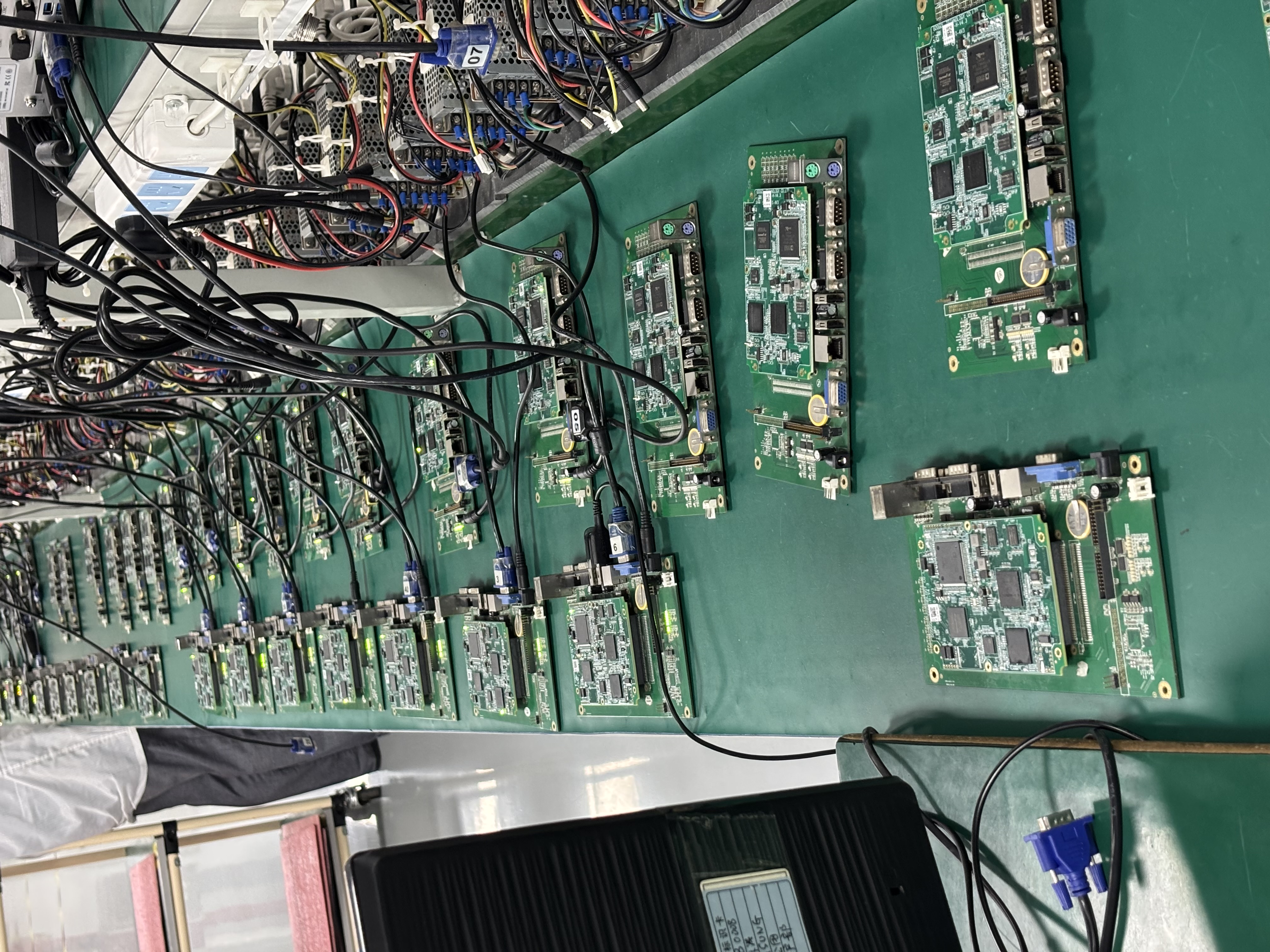
The entire machine adopts a low-power fanless architecture, with no cooling noise and no dust accumulation, perfectly adapting to the stringent clean, quiet, and long-term continuous operation environment of semiconductor cleanrooms. It also features a dual software and hardware fault tolerance mechanism, supporting abnormal fault self-locking, power-off position memory, and automatic reset alarms, minimizing the risk of wafer collision and damage and ensuring stable mass production on the production line.
IV. Core Differentiated Advantages of the Solution
- Highly Integrated All-in-One: A single board integrates three major functions: hard real-time motion control, high-speed vision acquisition, and edge AI detection. This replaces the traditional multi-device split architecture, reducing equipment volume by over 60% and significantly lowering the overall BOM cost and installation/debugging difficulty.
- Low Latency and High Synchronization: Pure FPGA hardware control provides nanosecond-level motion response. Motion and vision timing are hardware synchronized, with no system scheduling jitter, adapting to high-speed, high-precision semiconductor production scenarios.
- Native Edge AI Empowerment: Leveraging the RK3576's built-in NPU for localized defect detection eliminates the need for external industrial control equipment. It is lightweight, low power consumption, and easy to deploy, adapting to industrial edge intelligence upgrade requirements.
- Purely Domestic and Independently Controllable: The core master control and logic units are all domestic solutions, capable of completely replacing imported motion controllers + vision systems. This breaks foreign technology monopolies and adapts to the trend of domestic substitution for semiconductor equipment.
- Flexible Expansion and Customization: Supports multi-camera expansion, multi-machine collaborative scheduling, EtherCAT bus expansion, and MES production line integration, adapting to iterative upgrade requirements for different specifications of wafer transfer and inspection equipment.
V. Core Industry Application Scenarios
This solution is precisely adapted for semiconductor precision intelligent equipment, with core application scenarios as follows:
- 8/12-inch semiconductor wafer transfer robots and wafer loading/unloading manipulators.
- Integrated intelligent equipment for online inspection of semiconductor wafer appearance defects.
- Integrated automated equipment for precision handling, automatic alignment, and intelligent inspection in cleanrooms.
- Automated transfer equipment for semiconductor back-end packaging, testing, and sorting processes.
VI. Solution Summary
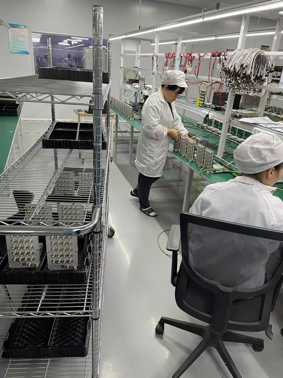
The domestic integrated solution based on RK3576+FPGA innovatively combines three core capabilities: FPGA hard real-time motion control, high-speed machine vision acquisition, and RK3576 edge AI intelligent detection. It thoroughly addresses the industry pain points of high latency, high cost, low integration, and insufficient intelligence in traditional semiconductor equipment's split architecture. The solution balances micron-level precision motion control performance with edge AI intelligent computing power, perfectly adapting to core scenarios of semiconductor wafer precision transfer and online defect detection. It offers advantages of low cost, high reliability, easy mass production, and customization, making it the preferred solution for the domestic and intelligent upgrade of semiconductor equipment.