Design of a PXIe Bus-Based Multi-Channel Parallel Data Acquisition System
Addressing the limitations and shortcomings of traditional data acquisition cards in terms of channel count, parallel data processing capability, and system real-time response, a PXIe bus-based multi-channel parallel data acquisition system was designed, using Xilinx's XC7A100T FPGA chip as the core processor. This system includes a data acquisition circuit, PXIe interface signal module, FIFO storage module, and power conversion circuit, among others. Tested results show that the system achieves a 200 KS/s sampling rate and multi-channel parallel data acquisition capabilities. It can upload data in real-time to the host computer for display via the PXIe bus. This system has high practical value and is significant for realizing the domestic production of low-cost PXIe acquisition cards.
Data acquisition technology is a key technology in the field of information technology, involving multiple aspects such as data capture, storage, processing, and transmission. To achieve fast and stable data transmission, the adoption of high-speed data transmission protocols has become increasingly important, and PXIe bus technology perfectly meets this demand. PXIe bus technology integrates the modular building characteristics of the PXI bus with the high-speed communication capabilities of the PCI Express bus, and adds timing and triggering bus functions, enabling it to effectively meet the requirements of modern test and measurement.
China is currently in the nascent stage of independent research and development of PXIe products. Domestic data acquisition functional modules show significant gaps compared to modules developed abroad in terms of sampling rate, resolution, and accuracy. For example, Yu Xixue et al. [1] proposed a data acquisition system combining LabVIEW and PXIe. Although this system addresses some transmission issues related to virtual instruments and big data, it suffers from high cost, system complexity, and stringent real-time requirements. Zhou Yangluo et al. [2] designed a new data acquisition system centered around the Kintex-7 chip. This system boasts a 5 GS/s sampling rate and 10-bit resolution. Although it offers strong anti-interference capabilities and good scalability, its real-time response in high-speed transmission still needs improvement. Shao Jingyi et al. [3] performed high-speed synchronous data acquisition for vacuum thermal tests based on the PXIe bus. While this method supports diverse test signal formats and high data accuracy, it has drawbacks such as demanding test environments, system complexity, and difficult maintenance.
Addressing the growing volume of data acquisition and the urgent need to improve the efficiency of data acquisition systems, this paper presents the development of a PXIe bus-based system with multi-channel parallel data acquisition and rapid data processing capabilities. This system is widely used in quality inspection processes in industrial automation production, where multi-channel parallel data acquisition enables quick and accurate retrieval of various product parameters. In environmental monitoring, the system can simultaneously acquire various environmental parameters such as temperature, humidity, and air quality, providing timely and comprehensive data support for environmental protection and disaster early warning. In medical device R&D, the system can perform high-precision acquisition and processing of complex physiological signals, providing critical basis for disease diagnosis and treatment plan formulation. Thus, the development of this system plays a positive role in promoting the advancement of domestic data acquisition systems and the localization of data acquisition cards.
1 Overall Design Scheme of the Acquisition System
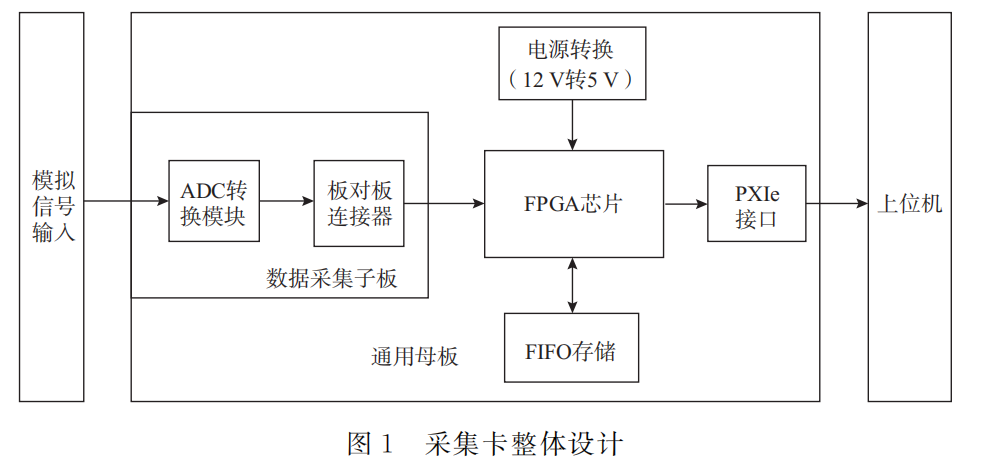
The data acquisition system designed in this paper primarily consists of two parts: a data acquisition daughterboard and a universal motherboard. The motherboard and daughterboard are connected via a board-to-board connector. The universal motherboard includes an FPGA core circuit, power conversion circuit, FIFO storage module, and PXIe interface module, among others. The overall process of the data acquisition system is as follows: a signal generator provides external analog signals to the acquisition daughterboard, which is responsible for acquiring these external analog input signals. These external signals are converted into digital signals by the ADC acquisition module. Subsequently, these digital signals are transmitted via the board-to-board connector to the FPGA processing system on the universal motherboard for data processing. Finally, the data is transmitted through the PXIe bus interface to the QT host computer for display. The block diagram of the acquisition system is shown in Figure 1.
2 System Software Design
The system software design in this paper primarily comprises three parts: PXIe interface logic design, AXI4 bus logic design, and data storage logic design. The PXIe interface logic design is responsible for communication between the system and the PXIe bus, including parsing the PXIe protocol, receiving and sending data, and data transmission with external devices. The AXI4 bus logic design is the core component for internal data transmission within the system, connecting various internal modules such as processors, memory, and peripherals. The data storage logic design is mainly responsible for managing and storing received data, including the implementation of storage controllers, data read/write operations, and allocation of storage resources.
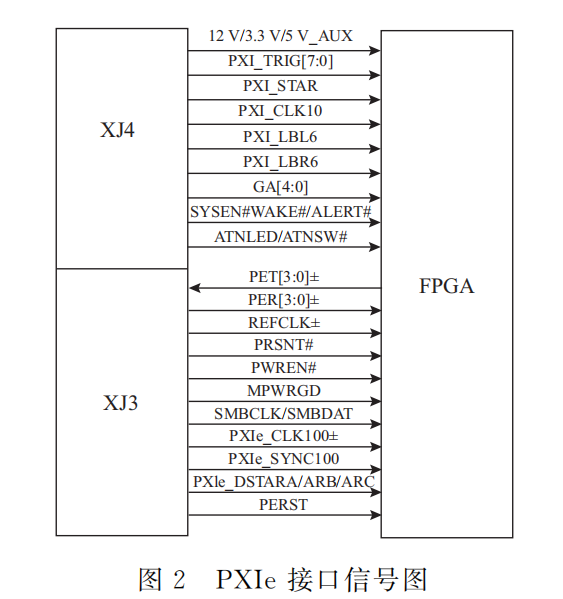
2.1 PXIe Interface Logic Design
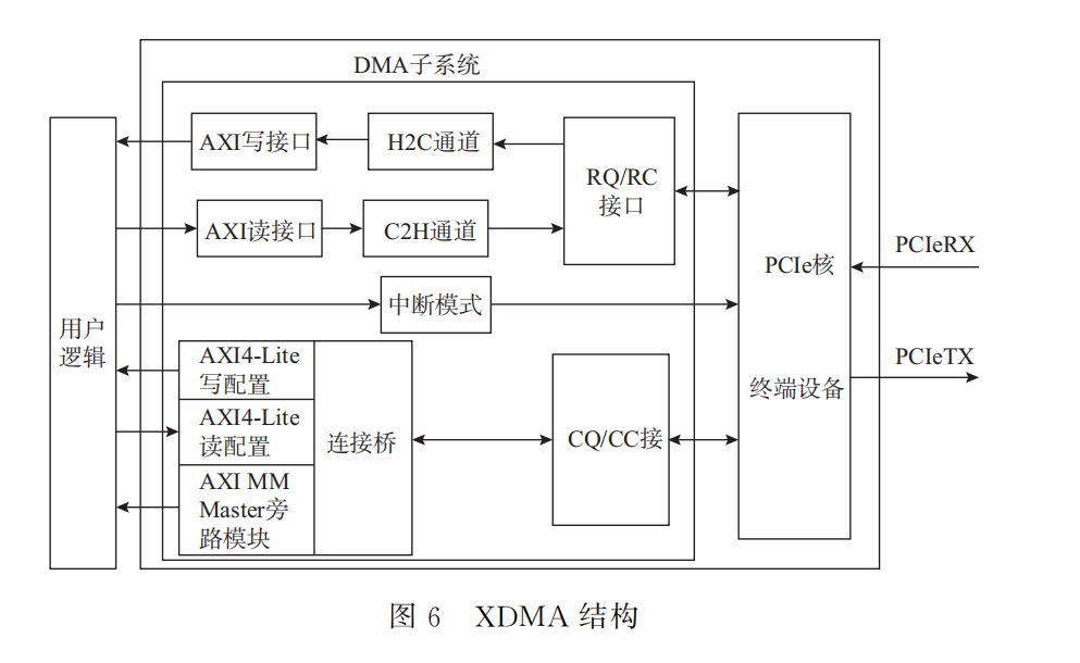
PXIe transmission methods are divided into PIO transmission and XDMA transmission. PIO transmission is suitable for scenarios with small data volumes, while XDMA transmission is suitable for high-speed transmission. Since this paper requires real-time transmission of system-acquired data, the XDMA transmission method was chosen. This paper adopts the Block Design method to construct the XDMA subsystem. FPGAs contain a large number of general-purpose IP cores, and with their continuous development and upgrades, using IP cores for program development is very convenient, requiring only subsequent IP core upgrades to update the code [11]. This design uses the AXI4 bus and XDMA core together to implement PCIe data link development, which is more convenient than building a data link using a PCIe IP core [12]. The XDMA structure is shown in Figure 6.
3.4 Matlab Data Analysis and Verification
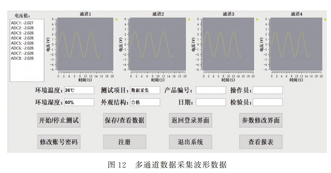
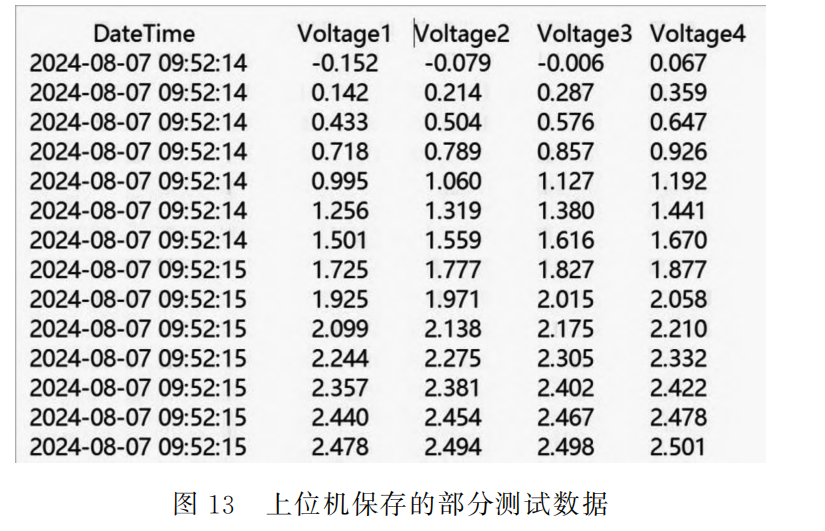
Using the data saving function in the host computer, the acquired data is saved to a file, yielding the acquired voltage data for four channels, as shown in Figure 13.
4 Conclusion
This paper presents the implementation of a PXIe bus-based multi-channel parallel data acquisition system. The system includes hardware acquisition circuits, FPGA logic programming, and a QT host computer program. The hardware circuits comprise a data acquisition circuit, PXIe interface signal module, FIFO storage module, and power conversion circuit, among others. The entire system describes the process of hardware circuit and software development and testing. After testing, it meets the design requirements, capable of multi-channel parallel data acquisition and transmission, possessing high application value and good scalability. The advanced nature of this system lies in its use of a high-performance FPGA chip, enabling multi-channel real-time parallel acquisition. Furthermore, it employs a high-bandwidth, low-latency PXIe interface data transmission bus, which offers higher transmission rates and better scalability compared to traditional PCI or other bus systems. In future research, further optimization of the system's hardware structure is needed to improve data acquisition accuracy and speed, and to expand the functionality of the host computer software to achieve more comprehensive data processing and analysis capabilities.