Design of an ARM+FPGA-Based Grating Data Acquisition Card
To ensure the accuracy of rotational inertia measurement, this paper designs a novel and advanced grating data acquisition card system using an FPGA chip and the Verilog HDL programming language. First, based on the overall system architecture design, multiple circuits such as the grating signal pre-processing circuit, FIFO data buffer circuit, and FPGA functional circuit are designed. Second, after completing the system's fabrication and debugging, equidistant and isochronous experiments are conducted on the system's grating signals. The results show that the FPGA-based grating data acquisition card designed in this paper features high accuracy, high stability, fast response speed, and stable and normal equidistant and isochronous sampling functions, ensuring the integrity and security of grating data, and meeting safe and reliable design standards. This research can provide important system support for precise rotational inertia measurement in the future.
As a new type of sensor, grating sensors are developed based on the Moiré fringe measurement principle. Using this sensor not only improves measurement accuracy but also achieves good response speed and anti-interference performance. The grating data acquisition card, as an important medium connecting the control system and the grating sensor, plays a crucial role [1]. However, traditional grating data acquisition cards suffer from issues such as a large number of discrete components, low stability, and poor security. To address this, this paper applies FPGA technology to design a novel and advanced grating data acquisition card system. This system primarily uses grating ruler displacement sensors, enabling high-precision, high-stability, and high-security measurements of objects such as rotational inertia, meeting the precise measurement needs of relevant enterprises [2].
1 Overall Architecture Design of the Data Acquisition Card System
To ensure the effectiveness of grating time and spacing control, the FPGA-based grating data acquisition card designed in this paper mainly comprises the following components: Grating Signal Reception Module, Field Programmable Gate Array (FPGA) Module, Peripheral Component Interconnect (PCI) Bus Interface Module, and First In First Out (FIFO) Data Buffer Module.
1.1 Grating Signal Reception Module
The design objective of the grating signal reception module is to divide four square wave signals into two orthogonal square wave signals through differential processing. When designing this module, a 50-line/mm Renishaw grating ruler and an MC3486 chip were selected. This chip offers advantages such as strong anti-interference, low cost, and high security, enabling scientific differential processing of four signals [3].
1.2 FPGA Module
In the design of the entire data acquisition card, an FPGA chip was primarily chosen for differential processing and counting of grating signals. This ensures that the system possesses grating signal identical-time control, identical-spacing control, and communication control functions, laying a solid foundation for precise acquisition of grating signal data in the future. Besides static memory, the FPGA module device also includes multiple components such as programmable units and logic cell arrays [4]. The application of the logic cell array module enables scientific configuration of the system's operating status. Furthermore, in the FPGA module, input/output modules are effectively connected to pins, and relevant parameters for input or output terminals are scientifically set in strict accordance with relevant standards and requirements. Concurrently, an appropriate amount of storage circuits were added and configured, and corresponding combinational logic circuits were designed in conjunction with the system's actual application requirements. To ensure the connection stability of each logic circuit, elements such as metal lines and switch matrices are also configured within the entire routing area. The FPGA module offers advantages such as simple and reasonable pin connections, low development cost, flexible and efficient development, and good compatibility [5].
1.3 PCI Bus Interface Module
During operation, this system can invoke a host computer to read and store interface data at high speeds, and the PCI bus interface is configured in a bus-based manner. The interface's clock frequency, width, and transmission speed are 33MHz, 32bit, and 264MB/s, respectively. The PCI bus is compatible with PCs and multiple peripheral devices, achieving a maximum transmission rate of 264MB/s, demonstrating high transmission performance. Therefore, in the specific design of this system, a PCI protocol chip was preferentially selected to reduce development costs and improve development efficiency.
1.4 FIFO Data Buffer Module
To enhance the data acquisition rate of this system, the IDT7206 chip was primarily chosen for designing and implementing the FIFO data buffer module. By expanding the depth and width of the IDT7206 chip, higher storage speeds can be achieved, providing users with various buffer service experiences such as full, empty, and half-full, meeting the demand for efficient data storage. Furthermore, when reading data using the IDT7206 chip in the FIFO data buffer module, data can be read directly after writing without the need to set address lines, simplifying the data buffering and reading process. Therefore, the IDT7206 chip is cost-effective, meeting the economic design requirements of the FIFO data buffer module.
2.1 Grating Signal Pre-processing Circuit Design
When selecting a grating for this system, the Renishaw grating ruler was preferentially chosen, as its output signal is a typical square wave. When designing the grating pre-processing circuit, technicians need to employ differential processing technology, combined with the characteristics of square wave signals, to divide the four signals into two. Additionally, the MC3486 chip was selected to convert the square wave signals from the original four channels to two channels. These two signals are then sent to the FPGA chip, where the FPGA chip performs unified processing on them, positively impacting the intelligent control of grating signal identical-time sampling data and identical-spacing sampling data in the future. The schematic diagram of the data acquisition card circuit is shown in Figure 1.
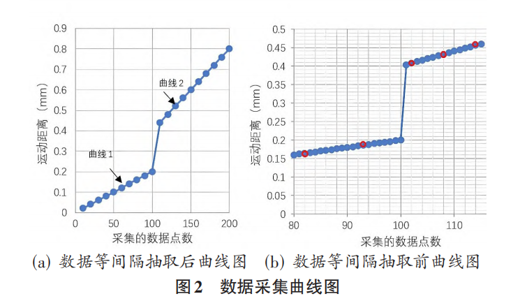
In this experiment, an isochronous data acquisition experiment was conducted on the grating signals using a rotational inertia measurement platform. The specific experimental procedure is as follows: The sampling time was set to 50 s, yielding the sampling results shown in Figure 3. By calculating each period, it was found that the standard deviation of the period reached 0.0013 s, indicating that applying this system for rotational inertia measurement can achieve high measurement accuracy.
Sienovo provides custom FPGA data acquisition card services.