How to Integrate Grating Sensors into an FPGA+ARM System?
Integrating grating sensors into an FPGA+ARM system requires hardware co-design and software architecture optimization to achieve high-precision real-time measurement. The core process is as follows:
🔌 I. Hardware Interface Design
-
Signal Conditioning Circuit
- Grating sensors output quadrature pulses (A/B phases) or four-channel sine signals. Differential receiver circuits must be designed to suppress common-mode noise, and shielded twisted-pair cables should be used for transmission to reduce electromagnetic interference.
- For sine signals, configure high-speed ADCs like AD9280 (125MSPS) to digitize the signals via FPGA.
-
FPGA Decoding Module
- Deploy hardware decoding logic in the FPGA:
- Quadrature frequency multiplication subdivision module: Resolution is increased by 4 times through dual-edge triggering (e.g., 0.5μm → 0.125μm).
- Direction determination circuit: Samples the B-phase level on the falling edge of the A-phase signal (B=1 for forward, B=0 for reverse).
- 32-bit high-speed counter: Records pulse counts in real-time, with overflow interrupts triggering ARM to read.
- Multi-channel expansion: Use 74HC4052 multiplexers to group and multiplex signals (e.g., 4 sensors/group), with FPGA polling to reduce pin usage.
- Deploy hardware decoding logic in the FPGA:
-
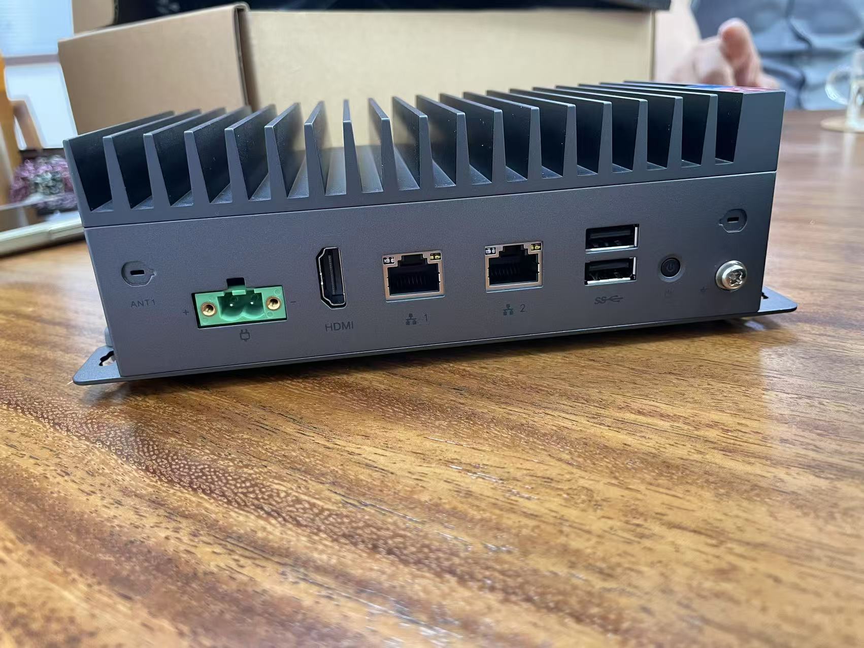
ARM-FPGA Communication Interface
- FSMC Parallel Bus: 16-bit data and address lines, 1GB/s bandwidth, configured in NOR Flash mode for register mapping.
- Ethernet Expansion: Connect to a Gigabit PHY chip via an RGMII interface, supporting EtherCAT multi-axis synchronization (≤±0.005mm synchronization error).
⚙️ II. FPGA Real-time Processing Layer
-
Timing Synchronization Design
- Global clock management: External crystal oscillator + PLL generate multiple clocks (e.g., 100MHz sampling clock, 120MHz SDRAM clock).
- Multi-sensor synchronization: Assign independent counters for each grating sensor channel, with a unified clear signal to align sampling start points.
-
Anti-interference Algorithm Hardening
- Adaptive notch filter: Filters out mechanical resonance frequencies in real-time (e.g., 50-200Hz), reducing acceleration errors caused by vibration.
- Dynamic tracking subdivision: In sine signal mode, calculates phase difference using the CORDIC algorithm, achieving 5nm micro-displacement resolution.
-
Data Preprocessing
- Displacement-to-acceleration conversion: Built-in nanosecond-level hardware timer calculates pulse interval time Δt, and outputs instantaneous acceleration (a=Δx/Δt²) combined with displacement difference Δx.
- Frame packing: Encapsulates multi-channel displacement/acceleration data into 32-bit data packets, and transfers them to ARM via DMA.
️ III. ARM Control Layer Implementation
-
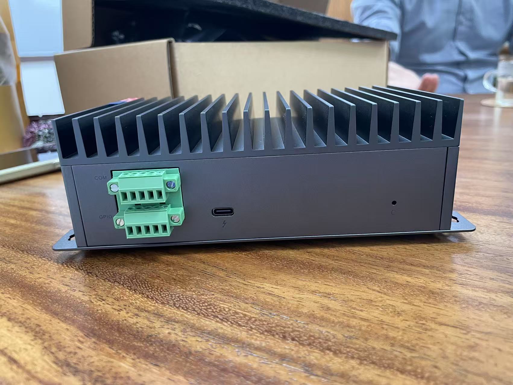
Drivers and Protocol Stack
- Grating protocol parsing: Supports encoder protocols such as EnDat2.2/BiSS-C, with decoding chips extended via SPI interface.
- Real-time operating system: Equipped with FreeRTOS, allocates high-priority tasks to handle motion control interrupts (response latency <10μs).
-
Core Algorithm Deployment
- Kalman Filtering: Fuses multi-sensor data to suppress random errors and improve positioning accuracy.
- Closed-loop Control: Generates PWM waves via PID algorithm, driving motors through the FPGA's SVPWM module to compensate for trajectory errors.
-
Communication and Interaction
- Data storage: DDR3 caches historical data, supporting USB export of CSV format records.
- Network interface: Custom lightweight UDP/IP core enables 10 Gigabit Ethernet (SFP+) for real-time upload of monitoring data.
️ IV. Debugging and Optimization Key Points
Item
Key Measures
PCB Electromagnetic Compatibility
Power/ground plane split design, grating signal routing on stripline layers, impedance matching 100Ω±10%
Multi-axis Synchronization Calibration
EtherCAT distributed clock synchronization, FPGA built-in timestamp counter (accuracy <5ns)
Low-Power Design
FPGA static power optimization (≤1W), ARM dynamic frequency scaling (168MHz → 48MHz standby)
Reliability Verification
Wide temperature testing (-40℃~+85℃), vibration table simulating mechanical shock (5-200Hz sweep)
⚠️ V. Typical Problem Solutions
- Signal Loss:
Add a three-stage flip-flop synchronization chain to eliminate metastability, use a hysteresis comparator to shape weak sine signals. - Multi-channel Crosstalk:
Photoelectric isolation + magnetic coupling isolation dual-protection design, independent ground plane segmentation between channels. - Long-Distance Transmission:
For 15-meter cable scenarios, switch to FBG fiber Bragg grating sensors, using CWDM wavelength demodulation to resist attenuation.
This solution utilizes a hierarchical architecture of grating signal hardware accelerated processing (FPGA) + intelligent control algorithms (ARM) to meet stringent application requirements such as ±1μm positioning for CNC machine tools and 5nm resolution for semiconductor inspection.