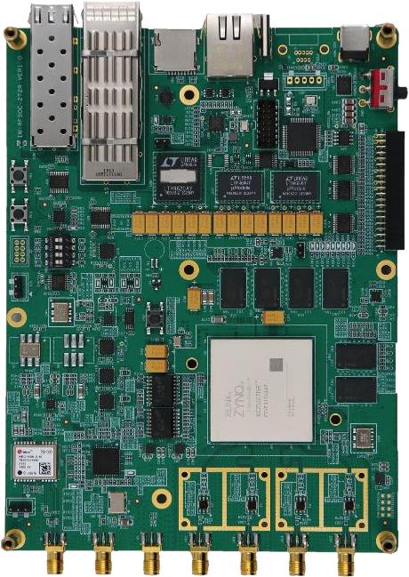
ZYNQ RFSoC Development Board - USRP Software Defined Radio X410mini Development Board - 5G Evaluation Board
RFSoC Development Board - USRP Software Defined Radio X410mini Development Board - 5G Evaluation Board
The Zynq® UltraScale+™ RFSoC ZCU208 Evaluation Kit is an ideal RF test platform for out-of-the-box evaluation and cutting-edge application development. The kit includes the UltraScale+ RFSoC ZU48DR, which integrates eight 14-bit 5GSPS ADCs, eight 14-bit 10GSPS DACs, and eight Soft-Decision Forward Error Correction (SD-FEC) cores, designed for rapid bring-up of RF-class applications.
Product Description
The Zynq® UltraScale+™ RFSoC ZCU208 Evaluation Kit is an ideal RF test platform for out-of-the-box evaluation and cutting-edge application development. The kit includes the Zynq UltraScale+ RFSoC ZU48DR, which integrates eight 14-bit 5GSPS ADCs, eight 14-bit 10GSPS* DACs, and eight Soft-Decision Forward Error Correction (SD-FEC) cores, designed for rapid bring-up of RF-class applications. By perfectly combining Arm® Cortex®-A53 and Cortex-R5 subsystems, programmable logic, and the highest signal processing bandwidth in a single Zynq UltraScale+ device, the ZCU208 Evaluation Kit is the most comprehensive RF analog-to-digital signal chain prototyping platform.
Target Applications:
-
Remote PHY for Cable Access
-
Early Warning Phased Array Radar / Digital Array Radar
-
Satellite Communications
-
5G Wireless
-
Test & Measurement
-
All High-Performance RF Applications
Key Features
Industry's Only Adaptive Single-Chip Radio Platform
- The Zynq UltraScale+ RFSoC XCZU48DR-2FSVG1517E chip is provided on the ZCU208 evaluation board.
- Integrates eight 5GSPS ADCs, eight 10GSPS* DACs, and eight SD-FEC design instances.
- Lidless package for enhanced thermal performance.
*10GSPS is achieved using the ZU48DR SCD5184 chip.
Equipped with all board-level features required for design development
- DDR4 Component – 4GB, 64-bit, 2666 MT/s, connected to Programmable Logic (PL)
- DDR4 SODIMM — 4GB, 64-bit, 2400MT/s, connected to Processing Subsystem (PS)
- FPGA Mezzanine Card (FMC+) interface for I/O expansion, including 12x 33Gb/s GTY transceivers and 34 user-defined differential I/O signals.
- Quad zSFP/zSFP+ module assembly
- 8 User I/Os, Monochrome LEDs
Includes reference design mezzanine cards to reduce development time
- CLK104 RF Clock Plug-in Card, displaying internal reference clock and external sampling clock.
- XM650 N79 Band Loopback Plug-in Card provides out-of-the-box simple loopback and example reference layouts for transceivers.
- XM655 Branch Plug-in Card allows for in-depth lab-based measurements, including Multi-Block Synchronization (MTS).
Development Board Specifications
| Value | |
|---|---|
| Height | 12.225 inch (31.05cm) |
| Width | 10.675 inch (27.11cm) |
| Thickness (+/-5%) | 0.119 inch (0.302cm) |
| Operating Ambient Temperature | 0◦C to +45◦C |
| Storage Ambient Temperature | –25◦C ~ +60◦C |
RF Data Converters
| Number of 14-bit RF-ADCs | 8 |
| Max Rate (GSPS) | 5 |
| Number of 14-bit RF-DACs | 8 |
| Max Rate (GSPS) | 10* |
| SD-FEC | 8 |
Memory
| PS DDR4 | 4GB 64-bit SODIMM |
| PL DDR4 | 8GB 64-bit Component |
| Micro SD Card | 16 GB |
| M.2 SATA Connector | ✓ |
| QSPI | 2 |
Communication & Networking
| USB (UART/JTAG) | 1 |
| RJ-45 | 1 |
| SFP28 | 4 |
| USB 3.0 | 1 |
Display
| DIP Switches | ✓ |
| LEDs | ✓ |
| Buttons | ✓ |
Expansion Connectors
| FMC+ | 1 |
| RFMC 2.0 | 2 |
Add-on Cards
| XM650 | 1 |
| XM655 | 1 |
| CLK104 | 1 |
Control & I/O
| I2C | ✓ |
| PMBUS | ✓ |
| JTAG PC4 Header | ✓ |
Boot Options
| SD Boot | ✓ |
| QSPI Boot | ✓ |
| JTAG Boot | ✓ |
Power Consumption
| 12V Wall Adapter | ✓ |
| ATX Power Supply Compatible | ✓ |
*10GSPS is achieved using the ZU48DR SCD5184 chip.