Design of a ZYNQ-based Four-Channel Data Acquisition System
Addressing the common issues of high cost and insufficient integration in existing receiver equipment, a low-cost, highly integrated four-channel ADS-B receiver is designed. This device is the first in the industry to integrate low-cost real-time signal acquisition, on-board multi-band ADS-B real-time decoding, and other functions into a single four-channel miniature RF receiver. The device uses a ZYNQ-7000 series chip as the main control chip, and the design includes an RF front-end receiver circuit module, a signal acquisition circuit module, a high-speed, large-capacity data storage module, etc., to achieve high-speed sampling and processing of target signals such as ADS-B. Test results show that the receiver can successfully receive and demodulate ADS-B long message signals, providing a low-cost, low-power overall solution for high-performance data acquisition and real-time signal processing.
Introduction
With the rapid development of the aviation industry, the issue of airspace flight safety has garnered attention. In aviation, Automatic Dependent Surveillance-Broadcast (ADS-B) is an avionics technology where an aircraft automatically broadcasts its position, altitude, identification number, and other relevant information while in the air [1]. ADS-B technology facilitates the management of aircraft status by relevant personnel and allows for avoidance of nearby aircraft, significantly enhancing safety and airspace traffic efficiency. Therefore, it is crucial for receiving equipment on aircraft to be able to receive aircraft data broadcast via ADS-B signals and decode the relevant information [2].
Currently used receiving devices, such as RTL-SDR [3-4], are inexpensive but only include an RF front-end and an 8-bit Analog-to-Digital Converter (ADC). They require a PC to demodulate baseband signals, leading to poor real-time performance and strong dependency. Highly integrated receivers like AD9371 [5] and AD9361 [6] are powerful, with a receiving signal range up to 6 GHz. However, for ADS-B signal reception alone, the AD9371 and AD9361 chips are relatively expensive and have redundant functionalities. Therefore, it is necessary to design a low-cost and highly integrated receiver specifically for ADS-B signals.
This paper proposes a ZYNQ-based four-channel ADS-B signal receiver. Each channel has a maximum sampling rate of 40 MSPS. It provides a complete solution from hardware circuit board design and logic control to data acquisition and processing, enabling efficient and low-cost ADS-B signal reception and processing, which has practical application significance in the aviation field.
1 Overall Design
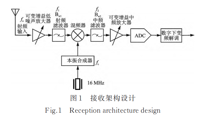
1.1 Receiver Architecture
To receive 1090 MHz ADS-B signals, receiver RF architectures typically choose between superheterodyne and zero-IF (direct conversion). Superheterodyne architecture offers advantages such as ease of design and convenient AD sampling, but also suffers from issues like image interference. While zero-IF architecture avoids image interference, it has drawbacks such as local oscillator (LO) leakage and I/Q imbalance. However, both receiver architectures inevitably suffer from I/Q imbalance, and I/Q sampling requires two ADCs, which places higher demands on hardware performance, making it difficult for actual hardware to meet I/Q balance and orthogonality requirements.
Digital intermediate frequency (IF) architecture can avoid the aforementioned problems. As shown in Figure 1, a digital IF receiver samples the analog IF signal based on a superheterodyne receiver, then performs digital down-conversion to demodulate the baseband signal, effectively avoiding I/Q imbalance issues. Furthermore, IF filtering is relatively easier for filters, which can lower the Q-factor requirements for filters and reduce overall system hardware cost.
1.3 Overall Design Scheme
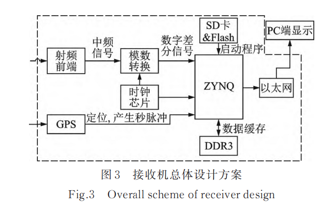
The overall design scheme of the receiver is shown in Figure 3. The system primarily consists of a ZYNQ-7000 main control module, an RF receiver module, an ADC module, a storage module, a clock module, and other components. The system's main control chip is a ZYNQ-7000 series chip, responsible for overall logic control and data processing. It receives ADS-B signals via an RF tuner, which are then down-converted to an IF signal. The analog-to-digital converter performs high-speed sampling of the IF signal [9], with a maximum sampling rate of 40 MS/s. The clock chip provides multiple selectable clock inputs for the ADC chip, and also provides clock input for the main control chip. To meet the requirements for real-time storage of acquired data, a high-speed, large-capacity DDR3 hardware circuit was designed, and an SD card stores the boot program. After data processing by the ZYNQ module, data can be uploaded to a PC via an Ethernet interface. The PC is only responsible for display and does not need to process data, which greatly improves the real-time performance of the receiver and reduces its reliance on the PC.
2.2 RF Module Design
The 1090 MHz ADS-B RF signal is received from the antenna. Signals attenuate after long-distance transmission, so the signals received by the antenna are relatively weak. Therefore, the signal is fed into a low-noise amplifier (LNA) for amplification, then into an RF bandpass filter to remove spurious signals and image interference. A local oscillator (LO) generation circuit produces the LO signal, which, along with the amplified and filtered signal, is fed into a mixer for frequency conversion. The mixed signal then passes through an IF filter, and then into an IF amplifier to boost its power. The IF amplifier provides the receiver's sensitivity and selectivity. Subsequent processing is performed at the IF, which also reduces processing costs.
The design, as shown in Figure 1, successfully eliminates reliance on external surface acoustic wave (SAW) filters, external LNAs, balun transformers, and low-dropout linear regulators. This ensures performance while minimizing cost in subsequent applications, and also provides greater flexibility. Internal RF automatic gain control (AGC) is introduced to ensure optimal signal-to-noise ratio (SNR) and minimal signal distortion. An embedded smart power detector adapts to different input power scenarios, optimizing RF performance and providing a special spurious-free dynamic range. In practical applications, as the RF input power changes, the internal power detector automatically adjusts the LNA gain to maintain optimal levels, ensuring the best IF output signal quality under all operating conditions.
In high-speed signal reception systems, the design of the RF front-end input circuit is crucial, requiring consideration of impedance matching, noise suppression, and other factors. Therefore, in the Printed Circuit Board (PCB) design, the RF input lines for all four channels employ 70 Ω impedance matching. The RF receiver module achieves low power consumption and high RF performance in system applications, offering superior performance in terms of RF sensitivity, linearity, and adjacent channel interference rejection.
2.3 ADC Module Circuit Design
Based on analysis, the ADC sampling rate is set to 24 MHz. The ADC module uses the AD9219 chip, which has a maximum sampling rate of 40 MSPS, fully meeting the requirements. Furthermore, the chip integrates various functional features, ensuring flexibility and reducing system cost, meeting the four-channel requirements while providing sufficient sampling rate at a lower cost.
4 System Test and Verification
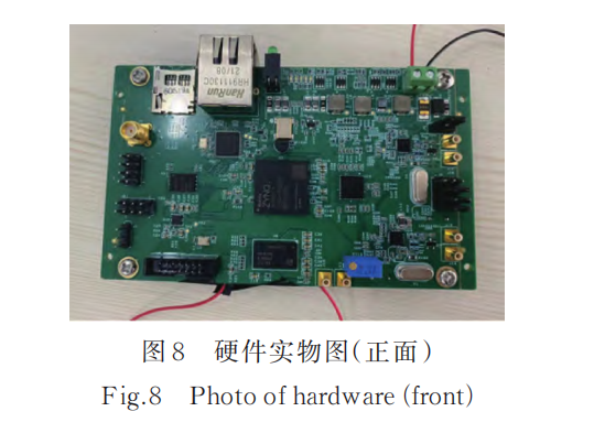
The front view of the physical hardware for the ADS-B signal data acquisition system is shown in Figure 8. It is an 8-layer PCB board measuring 10 cm × 6.9 cm. The overall chip cost is low, making it a small-volume, low-cost design solution.
To verify the power consumption of the receiver, an adjustable power supply provided 5 V voltage and a rated current of 1 A. After an 8-hour test, the receiver's power consumption was measured to be no more than 4 W. Compared to other ADS-B receivers, such as the one in reference [14] with power consumption not exceeding 5 W [14], this represents a 20% reduction in power consumption.
To verify if the receiver can receive real-time ADS-B signals, the real-time collected data from the receiver was processed and sent to a PC for display using Matlab. Figure 9 shows the real-time received signals, with signals identified