AI Server PCIe Switch Interconnect Chip Technology: Domestic Alternatives to Broadcom Solutions
AI Servers: A Deep Dive into Interconnect Chip Technology
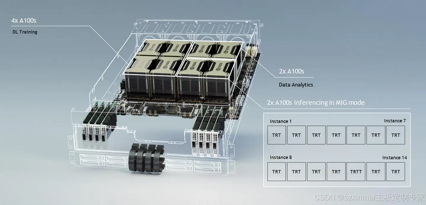
Shenzhen Xinmai provides custom board card services for Zhongxingwei PCIe Switch AI server interconnect chips.
As large language models and generative AI workloads demand increasingly dense GPU clusters, the silicon connecting those GPUs to each other and to the host CPU has become just as strategically important as the GPUs themselves. This article walks through the three principal interconnect layers inside a modern AI server — PCIe Switch and Retimer chips for CPU-GPU links, NVLink and NVSwitch for GPU-to-GPU fabric, and memory interface chips for CPU-DRAM bandwidth — and surveys the competitive landscape for domestic Chinese alternatives to the Broadcom-dominated status quo.
According to TrendForce data, AI server shipments reached approximately 130,000 units at the time of writing, accounting for about 1% of global server shipments. With Microsoft, Meta, Baidu, and ByteDance all aggressively adding capacity to support generative AI products, the annual growth rate of AI server shipments in 2023 was projected to reach 15.4%, and AI servers were forecast to grow at a compound annual growth rate (CAGR) of 12.2% from 2023 to 2027.
Inside the NVIDIA DGX H100: A Reference Architecture
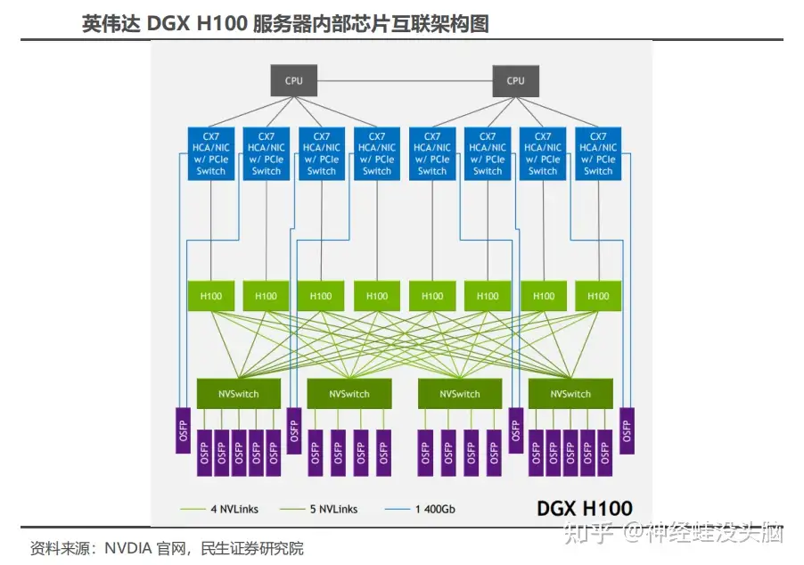
The DGX H100, launched in 2022, is the latest iteration of NVIDIA's DGX system and the foundation of NVIDIA DGX SuperPOD. The server is equipped with 8 H100 GPUs, packs 640 billion transistors, delivers 6× the AI performance of the previous generation at the new FP8 precision, and provides 900 GB/s of GPU-to-GPU bandwidth.
Inside the DGX H100, the blue blocks visible in system diagrams are InfiniBand / Ethernet adapters (ConnectX-7, or CX7). Each CX7 can act simultaneously as a network interface card and a PCIe Switch expansion device, bridging the CPU and H100 GPUs over PCIe 5.0. Four CX7 chips are assembled onto a single dual-slot card, and each card exposes two 800G OSFP optical module ports. GPU-to-GPU communication within a single DGX H100 node runs over NVLink. Each H100 GPU has 18 NVLink ports; each link delivers 50 GB/s bidirectional bandwidth, giving 18 × 50 GB/s = 900 GB/s total bidirectional bandwidth per GPU. That bandwidth is distributed across four on-board NVSwitch chips, with each NVSwitch connecting to 4–5 OSFP optical modules (18 total per node). Each OSFP module uses 8 optical lanes at 100 Gbps per lane, yielding 800 Gbps per module.
1. CPU–GPU Interconnect: PCIe Switch and Retimer Chips
What Is a PCIe Switch?
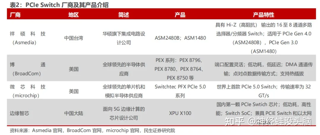
PCIe Switch chips — sometimes called PCIe crossbar switches or PCIe fabric devices — allow multiple PCIe endpoints to share a single upstream PCIe port. Because PCIe is inherently a point-to-point protocol, a Switch is the mechanism through which one CPU root complex can fan out to many GPUs, NVMe SSDs, or network adapters without running out of CPU-side PCIe lanes. PCIe Switches have been deployed in enterprise storage arrays for years and are now a standard component in GPU server platforms.
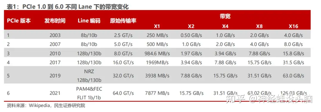
PCIe Generation History and Bandwidth Growth
PCIe traces its lineage to Intel's "3GIO" proposal from 2001, which was ratified by the PCI Special Interest Group (PCI-SIG) and renamed PCI Express in 2002.
| Generation | Year | Transfer Rate | Per-Lane Bandwidth |
|---|---|---|---|
| PCIe 1.0 | 2003 | 2.5 GT/s | 250 MB/s |
| PCIe 2.0 | 2007 | 5 GT/s | 500 MB/s |
| PCIe 3.0 | 2010 | 8 GT/s | ~985 MB/s |
| PCIe 4.0 | 2017 | 16 GT/s | ~1.97 GB/s |
| PCIe 5.0 | 2019 | 32 GT/s | ~3.94 GB/s |
| PCIe 6.0 | 2022 | 64 GT/s | ~7.88 GB/s |
PCIe 6.0, formally published by PCI-SIG in 2022, doubles transfer rate to 64 GT/s by adopting PAM4 (Pulse-Amplitude Modulation 4-level) signaling in place of NRZ, allowing higher data density per symbol at the cost of tighter signal-integrity margins — which is precisely why Retimer chips have become mandatory at longer trace lengths.
Market Size
According to QYResearch, global PCIe chip market revenue reached USD 790 million in 2021 and is forecast to reach USD 1.8 billion by 2028, a CAGR of 11.9%. China is the single largest market for PCIe Switch chips, driven by hyper-scale data center build-outs for cloud computing, big data, and AI applications.
PCIe Retimer Chips: Signal Integrity at High Speeds
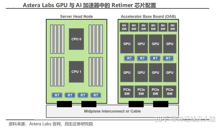
As PCIe moves to Gen 5 and Gen 6 speeds, board traces longer than a few centimetres accumulate enough insertion loss and crosstalk to corrupt signals before they reach the far-end receiver. A Retimer (sometimes called a redriver with full clock-data recovery) fully re-times and re-drives the signal, effectively resetting the channel budget. In a dense AI server, at least one Retimer is required between the CPU and each GPU to guarantee signal integrity. Many AI accelerator designs use four or more Retimers; Astera Labs, for example, configures four Retimer chips in its AI accelerator reference design.
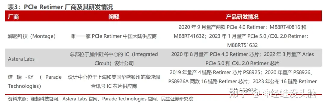
Competitive Landscape for PCIe Retimers
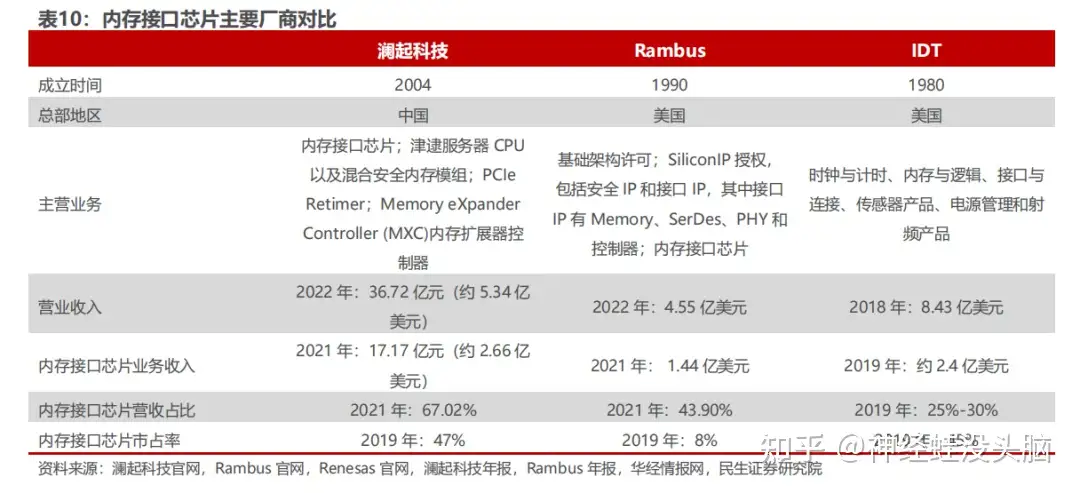
Three companies currently lead the PCIe Retimer market: Parade Technologies (謙瑞-KY), Astera Labs, and Montage Technology (澜起科技).
Montage Technology entered the PCIe space earliest among Chinese mainland vendors. It is the only Chinese mainland supplier capable of mass-producing PCIe 4.0 Retimers, and its PCIe 5.0 Retimer development was reported to be progressing well at the time of writing.
Additional players pursuing PCIe Retimer products include:
- Renesas — offers two PCIe 3.0 Retimer products: the 89HT0816AP and the 89HT0832P.
- Texas Instruments — offers the DS160PT801, a 16 Gbps, 8-channel PCIe 4.0 Retimer.
- Microchip Technology — launched the XpressConnect Retimer series in November 2020, supporting PCIe 5.0 at 32 GT/s.
2. GPU-to-GPU Interconnect: NVLink and NVSwitch
While PCIe handles the CPU-to-GPU path, GPU cluster performance hinges on GPU-to-GPU bandwidth — and PCIe is far too slow for all-reduce operations across 8 or more high-end GPUs. NVIDIA's answer is NVLink and NVSwitch. Competing approaches from other vendors include AMD's Infinity Fabric and Intel's CXL (Compute Express Link).
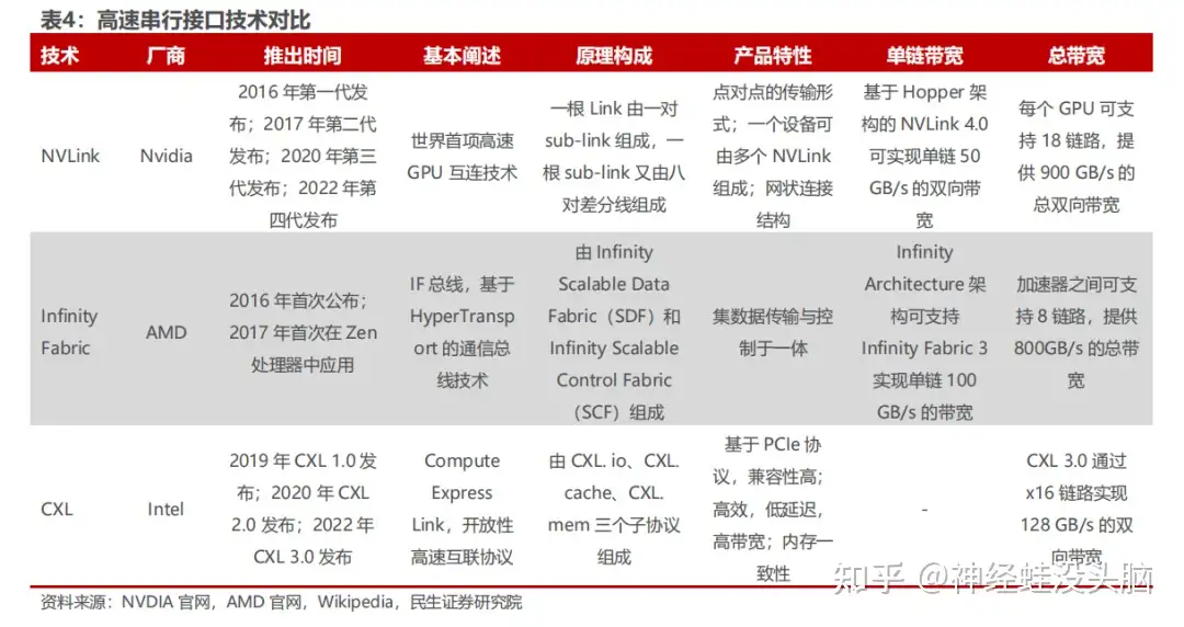
NVLink Generation History
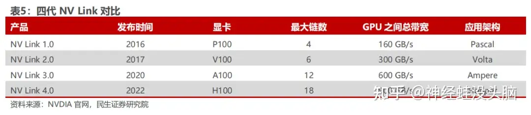
NVLink was first introduced alongside the Pascal GP100 GPU in 2016, using High-Speed Signaling interconnect (NVHS) technology and NRZ differential signaling.
| Generation | Architecture | Year | Bandwidth per Link (Bidirectional) | Max Links per GPU | Total GPU Bandwidth |
|---|---|---|---|---|---|
| NVLink 1.0 | Pascal | 2016 | 40 GB/s | 4 | 160 GB/s |
| NVLink 2.0 | Volta | 2017 | 50 GB/s | 6 | 300 GB/s |
| NVLink 3.0 | Ampere | 2020 | 50 GB/s | 12 | 600 GB/s |
| NVLink 4.0 | Hopper | 2022 | 50 GB/s | 18 | 900 GB/s |
The fourth-generation NVLink on the Hopper H100 adopts PAM4 modulation — the same signaling change seen in PCIe 6.0 — to maintain 50 GB/s per link while scaling to 18 links per chip.
NVSwitch: Scaling the GPU Fabric
NVLink on its own is point-to-point. NVSwitch is the crossbar fabric chip that connects multiple GPUs in an all-to-all topology, enabling any GPU to communicate with any other GPU at full NVLink bandwidth without traversing the CPU.
NVIDIA introduced the first-generation NVSwitch in 2018, manufactured on TSMC 12 nm FinFET, with 18 NVLink 2.0 ports. A single DGX V100 could use 12 NVSwitch chips to connect 16 V100 GPUs at full NVLink speed.
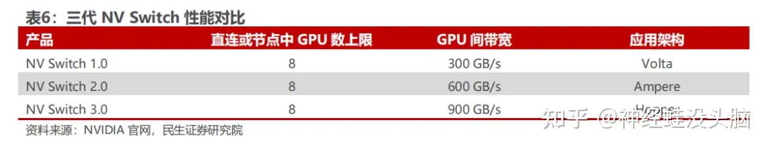
The third-generation NVSwitch, used in DGX H100 and HGX H100 systems, is manufactured on TSMC's 4N process. Each chip provides 64 NVLink 4.0 ports and enables GPU-to-GPU communication at 900 GB/s. A pool of GPUs interconnected through NVSwitch can collectively act as a single logical accelerator, which is the architectural basis for NVIDIA's multi-node NVLink Switch fabric announced for future platforms.
3. CPU-to-DRAM Interconnect: Memory Interface Chips
Why Servers Need Memory Interface Chips
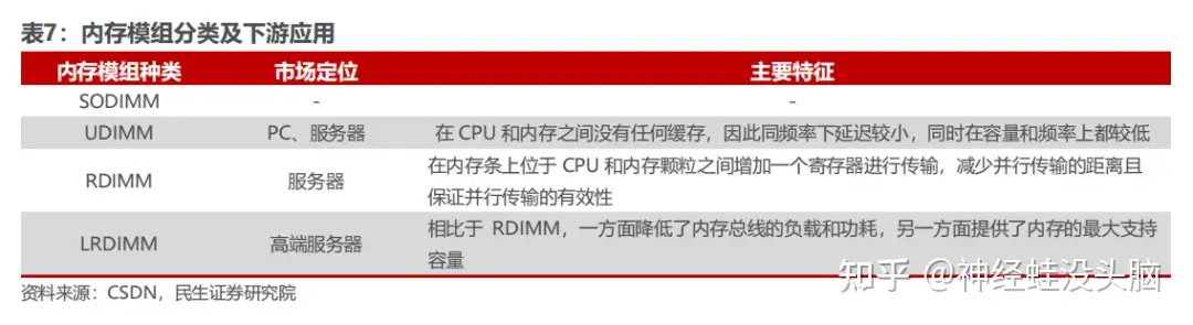
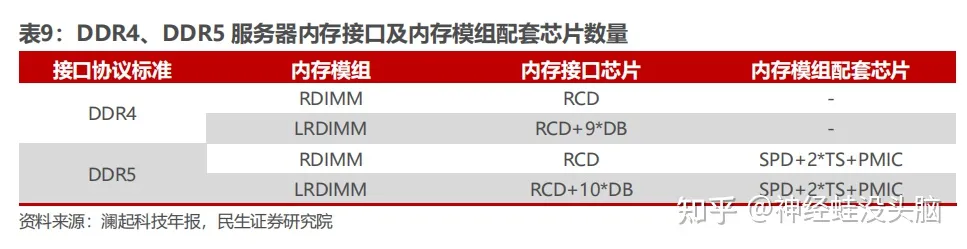
Server memory modules are predominantly RDIMM (Registered DIMM) or LRDIMM (Load-Reduced DIMM) form factors, both of which interpose a buffer chip between the memory controller and the DRAM dies. Unlike consumer UDIMMs, server DIMMs require ECC, stable signal integrity at higher ranks, and low idle power. Memory interface chips — the Register Clock Driver (RCD) and Data Buffer (DB) — are the core logic devices in these modules.
- RCD (Register Clock Driver): buffers address, command, and control signals from the memory controller, preventing the controller output from loading excessively as rank count increases.
- DB (Data Buffer): buffers read and write data signals between the controller and the DRAM dies, used in LRDIMM configurations to decouple data bus loading entirely.
DDR4 to DDR5 Transition
DDR4 became the dominant server memory standard in 2016. The JEDEC standard body progressively tightened DDR4 interface chip specifications across four sub-generations (Gen 1.0, Gen 1.5, Gen 2.0, and Gen 2plus), with the final Gen 2plus products reaching a maximum transfer rate of 3200 MT/s.
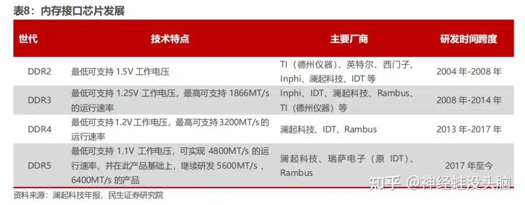
DDR5 memory interface chips are currently planned across three sub-generations:
| Sub-Generation | Max Transfer Rate |
|---|---|
| DDR5 Gen 1 | 4800 MT/s |
| DDR5 Gen 2 | 5600 MT/s |
| DDR5 Gen 3 | 6400 MT/s |
Industry observers expected one to two additional sub-generations beyond DDR5 Gen 3. DDR5 Gen 1 interface chips command a higher per-unit price than DDR4 equivalents due to the increased design complexity required to meet tighter timing margins and the new power management architecture introduced in the DDR5 standard.
Market Growth
Global memory interface chip market revenue was approximately USD 280 million in 2016 and grew to approximately USD 570 million by 2018, a three-year CAGR of roughly 40%. The transition to DDR5 — with higher complexity driving higher ASPs and broadening adoption across both servers and PCs — is expected to sustain strong market growth.
Consolidated Market: Three Suppliers Worldwide
Memory interface chips are among the most technically demanding products in server silicon. Every chip must pass rigorous co-validation with the CPU vendor (Intel or AMD), the DRAM manufacturer, and the OEM server builder before volume production can begin. That qualification cycle, combined with the need to track multiple JEDEC specification revisions simultaneously, has systematically eliminated smaller players. The field contracted from more than ten competitors in the DDR2 era to just three by DDR4:
- Montage Technology (澜起科技) — China's only mass-production supplier of DDR5 Gen 1 memory interface chips.
- Renesas Electronics (formerly IDT) — a long-established supplier across multiple DDR generations.
- Rambus — holds significant patent portfolios and shipping silicon for DDR5.
For the DDR5 first sub-generation, only these three companies worldwide can supply production-qualified parts — a structural moat that makes memory interface chips one of the highest-barrier segments in the entire server chip ecosystem.
Summary
The interconnect silicon stack inside an AI server spans three distinct layers, each with its own technology trajectory and competitive dynamics:
- PCIe Switch and Retimer chips handle CPU-to-GPU links. The market is growing at ~12% CAGR and is currently dominated by a small number of US and Taiwanese vendors, with Montage Technology as the most mature Chinese mainland Retimer supplier.
- NVLink and NVSwitch form NVIDIA's proprietary GPU-to-GPU fabric, currently in its fourth generation at 900 GB/s per GPU. AMD's Infinity Fabric and Intel's CXL provide partial alternatives on competing platforms.
- Memory interface chips (RCD and DB) sit on every server DIMM and are now transitioning from DDR4 to DDR5. The global supply base has consolidated to three vendors, with Montage Technology holding the sole Chinese mainland position.
For system integrators and platform designers, each of these layers represents both a procurement dependency and a technology risk — and the push for domestic Chinese alternatives across all three segments is a defining strategic thread in the AI infrastructure buildout of this decade.