Cost-Effective Algorithm Acceleration Platform for Lattice FPGA + PCIe + x86 Servers
Edge-AI workloads and industrial computing tasks increasingly demand hardware acceleration that balances cost, flexibility, and deployment simplicity. This post introduces a platform built around the Lattice ECP5 FPGA paired with a PCIe Gen 3.0 interface, designed to drop into standard x86 server infrastructure and accelerate custom algorithms under Ubuntu or Windows — without the licensing overhead and power draw of larger, higher-cost FPGAs.
Why Lattice ECP5 for Algorithm Acceleration?
Lattice Semiconductor's ECP5 family occupies a practical middle ground in the FPGA market. Unlike high-end devices from Intel (Altera) or AMD (Xilinx), the ECP5 is optimized for low-power, cost-sensitive applications while still offering a meaningful complement of logic cells, DSP slices, and high-speed SERDES transceivers. For algorithm acceleration tasks — image preprocessing, protocol offload, signal processing pipelines, or inference on lightweight models — the ECP5 provides enough fabric to be useful without requiring the power budget or upfront cost of a data-center-class FPGA.
The ECP5 SERDES capability is particularly relevant here: it enables the PCIe physical layer, allowing the FPGA card to present itself as a standard PCIe endpoint to any x86 host, whether that host is running Ubuntu or Windows Server.
The ECP5 Versa Development Board
The hardware anchor for this platform is the ECP5™ Versa Development Board, Lattice's own reference design for evaluating the ECP5 FPGA family. It comes in a half-length PCIe form factor, meaning it fits in standard server and workstation slots without requiring a full-length slot — a practical advantage in dense rack deployments.
Figure 1. ECP5 Versa Development Board, Top Side
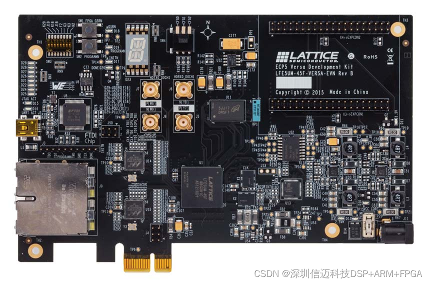
The board's feature set covers the key interfaces an engineer needs to prototype and validate an acceleration design:
- Half-length PCI Express form-factor — demonstrates PCIe x1 interconnection to the host CPU, giving designers a working PCIe endpoint to develop DMA engines and host-side drivers against
- Full-duplex SERDES channel via SMA connections — exposes one SERDES lane for electrical characterization and loopback testing, useful for validating signal integrity before committing a custom board design
- USB-B for UART and device programming — provides a single-cable path for both debug console access and JTAG/SPI programming, simplifying the bench setup
- Dual RJ45 Gigabit Ethernet (RGMII) — two independent 10/100/1000 Ethernet ports allow the FPGA to bridge, process, or inspect network traffic without touching the host CPU's NICs
- 128 MB SPI Boot Flash — stores the FPGA configuration bitstream so the board comes up autonomously on power-on, without requiring host-side programming at each boot
- DDR3-1866 memory (64 Mb × 16) — provides off-chip buffering for data-intensive algorithms that exceed the FPGA's internal block RAM
- Expansion mezzanine connector — allows custom daughter cards for domain-specific I/O (sensors, custom interfaces, additional memory)
- 14-segment alphanumeric display, switches, and LEDs — onboard debug aids for demonstrating state and status during development without requiring a full software stack
- Diamond® programming support — integrates with Lattice's Diamond IDE for bitstream synthesis, place-and-route, and device programming
- On-board reference clock sources — provides stable clocking for both the FPGA fabric and the PCIe/SERDES subsystems
PCIe Gen 3.0 and the x86 Integration Story
The platform targets PCIe Gen 3.0, which provides sufficient bandwidth for bulk data transfer between the host CPU and the FPGA accelerator. In a typical deployment, the x86 host enqueues work descriptors and input data over PCIe DMA, the FPGA processes the data in its custom algorithm pipeline, and results are DMA'd back to host memory. The host-side driver stack runs on standard Linux (Ubuntu) or Windows, making integration straightforward for engineering teams already familiar with PCIe device driver development.
Because ECP5 implements the PCIe endpoint in SERDES logic (not a hard PCIe IP block), the design is flexible — the PCIe link parameters, endpoint configuration space, and DMA engine behavior can all be customized in HDL. This matters for niche acceleration workloads where a fixed-function PCIe IP might impose unnecessary overhead or constrain the data path.
Evaluation and Deployment with Sienovo
For teams that want to validate whether this platform fits their algorithm before committing engineering resources, Sienovo (信迈) provides algorithm evaluation and hardware evaluation solutions around this ECP5 + PCIe platform. This covers both the FPGA-side HDL implementation and the host-side integration work, giving customers a complete proof-of-concept rather than just a development board. Industrial computing applications — edge inference, vision preprocessing, protocol acceleration — are the primary target, particularly where a cost-effective, server-resident FPGA accelerator is preferable to a discrete GPU or a higher-power FPGA card.